
The vast majority of solid substances like high temperature superconductors, biocompatible plastics, silicon chips, etc. are destined to play an ever expanding role in future development of science.
After studying this Unit, you will be able to
From our earlier studies, we know that liquids and gases are called fluids because of their ability to flow. The fluidity in both of these states is due to the fact that the molecules are free to move about. On the contrary, the constituent particles in solids have fixed positions and can only oscillate about their mean positions. This explains the rigidity in solids. These properties depend upon the nature of constituent particles and the binding forces operating between them. The correlation between structure and properties helps in the discovery of new solid materials with desired properties. For example, carbon nanotubes are new materials that have potential to provide material that are tougher than steel, lighter than aluminium and have more conductive property than copper. Such materials may play an expanding role in future development of science and society. Some other materials which are expected to play an important role in future are high temperature superconductors, magnetic materials, biodegradable polymers for packaging, biocompliant solids for surgical implants, etc. Thus, the study of this state becomes more important in the present scenario.
In this Unit, we shall discuss different possible arrangements of particles resulting in several types of structures and explore why different arrangements of structural units lend different properties to solids. We will also learn how these properties get modified due to the structural imperfections or by the presence of impurities in minute amounts.
In Class XI you have learnt that matter can exist in three states namely, solid, liquid and gas. Under a given set of conditions of temperature and pressure, which of these would be the most stable state of a given substance depends upon the net effect of two opposing factors. These are intermolecular forces which tend to keep the molecules (or atoms or ions) closer, and the thermal energy, which tends to keep them apart by making them move faster. At sufficiently low temperature, the thermal energy is low and intermolecular forces bring them so close that they cling to one another and occupy fixed positions. These can still oscillate about their mean positions and the substance exists in solid state. The following are the characteristic properties of the solid state:
(i) They have definite mass, volume and shape.
(ii) Intermolecular distances are short.
(iii) Intermolecular forces are strong.
(iv) Their constituent particles (atoms, molecules or ions) have fixed positions and can only oscillate about their mean positions.
(v) They are incompressible and rigid.
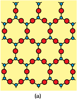
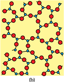
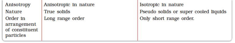
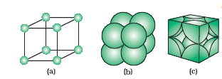
Solids can be classified as crystalline or amorphous on the basis of the nature of order present in the arrangement of their constituent particles. A crystalline solid usually consists of a large number of small crystals, each of them having a definite characteristic geometrical shape. The arrangement of constituent particles (atoms, molecules or ions) in a crystal is ordered and repetitive in three dimensions. If we observe the pattern in one region of the crystal, we can predict accurately the position of particles in any other region of the crystal however far they may be from the place of observation. Thus, crystal has a long range order which means that there is a regular pattern of arrangement of particles which repeats itself periodically over the entire crystal. Sodium chloride and quartz are typical examples of crystalline solids. Glass, rubber and many plastics do not form crystals when their liquids solidify on cooling. These are called amorphous solids. The term amorphous comes from the Greek word amorphos, meaning no form.The arrangement of constituent particles (atoms, molecules or ions) in such a solid has only short range order. In such an arrangement, a regular and periodically repeating pattern is observed over short distances only. Regular patterns are scattered and in between the arrangement is disordered. The structures of quartz (crystalline) and quartz glass (amorphous) are shown in Fig. 1.1 (a) and (b) respectively. While the two structures are almost identical, yet in the case of amorphous quartz glass there is no long range order.
The structure of amorphous solids is similar to that of liquids. Due to the differences in the arrangement of the constituent particles, the two types of solids differ in their properties.
Crystalline solids have a sharp melting point. At a characteristic temperature they melt abruptly and become liquid. On the other hand, amorphous solids soften, melt and start flowing over a range of temperature and can be moulded and blown into various shapes. Amorphous solids have the same structural features as liquids and are conveniently regarded as extremely viscous liquids. They may become crystalline at some temperature. Some glass objects from ancient civilisations are found to become milky in appearance because of some crystallisation. Like liquids, amorphous solids have a tendency to flow, though very slowly. Therefore, sometimes these are called pseudo solids or super cooled liquids.
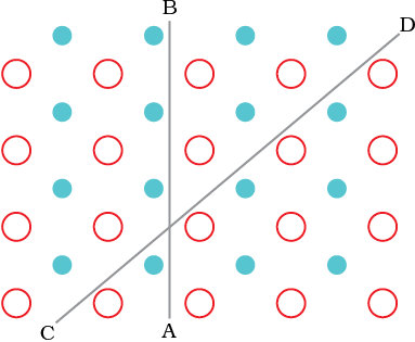
Fig. 1.2: Anisotropy in crystals is due to different arrangement of particles along different directions.
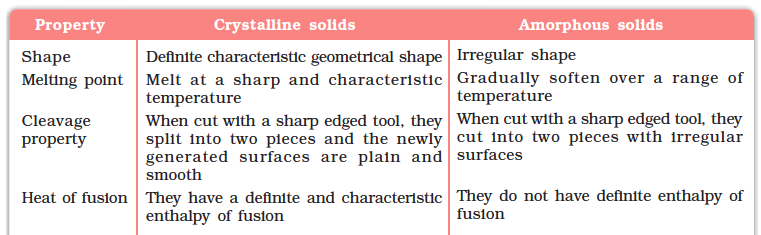
Crystalline solids are anisotropic in nature, that is, some of their physical properties like electrical resistance or refractive index show different values when measured along different directions in the same crystals. This arises from different arrangement of particles in different directions. This is illustrated in Fig. 1.2. This figure shows a simple two-dimensional pattern of arrangement of two kinds of atoms. Mechanical property such as resistance to shearing stress might be quite different in two directions indicated in the figure. Deformation in CD direction displaces row which has two different types of atoms while in AB direction rows made of one type of atoms are displaced. The differences between the crystalline solids and amorphous solids are summarised in Table 1.1.
Table 1.1: Distinction between Crystalline and Amorphous Solids
Besides crystalline and amorphous solids, there are some solids which apparently appear amorphous but have microcrystalline structures. These are called polycrystalline solids. Metals often occur in polycrystalline condition. Individual crystals are randomly oriented so a metallic sample may appear to be isotropic even though a single crystal is anisotropic.
Amorphous solids are useful materials. Glass, rubber and plastics find many applications in our daily lives. Amorphous silicon is one of the best photovoltaic material available for conversion of sunlight into electricity.
1.1 Why are solids rigid?
1.2 Why do solids have a definite volume?
1.3 Classify the following as amorphous or crystalline solids: Polyurethane, naphthalene, benzoic acid, teflon, potassium nitrate, cellophane, polyvinyl chloride, fibre glass, copper.
1.4 Refractive index of a solid is observed to have the same value along all directions. Comment on the nature of this solid. Would it show cleavage property?
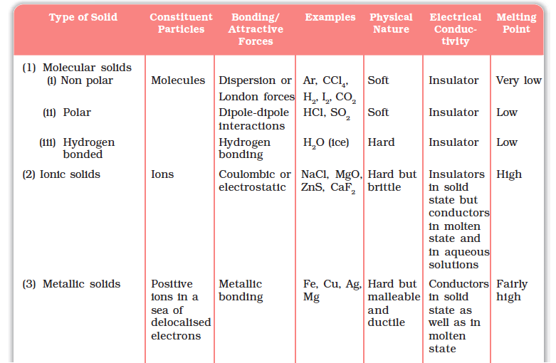
(i) Non polar Molecular Solids: They comprise either atoms, for example, argon and helium or the molecules formed by non polar covalent bonds, for example, H2, Cl2 and I2. In these solids, the atoms or molecules are held by weak dispersion forces or London forces about which you have learnt in Class XI. These solids are soft and non-conductors of electricity. They have low melting points and are usually in liquid or gaseous state at room temperature and pressure.
(ii) Polar Molecular Solids: The molecules of substances like HCl, SO2, etc. are formed by polar covalent bonds. The molecules in such solids are held together by relatively stronger dipole-dipole interactions. These solids are soft and non-conductors of electricity. Their melting points are higher than those of non polar molecular solids yet most of these are gases or liquids under room temperature and pressure. Solid SO2 and solid NH3 are some examples of such solids.
(iii) Hydrogen Bonded Molecular Solids: The molecules of such solids contain polar covalent bonds between H and F, O or N atoms. Strong hydrogen bonding binds molecules of such solids like H2O (ice). They are non-conductors of electricity. Generally they are volatile liquids or soft solids under room temperature and pressure.
Ions are the constituent particles of ionic solids. Such solids are formed by the three dimensional arrangements of cations and anions bound by strong coulombic (electrostatic) forces. These solids are hard and brittle in nature. They have high melting and boiling points. Since the ions are not free to move about, they are electrical insulators in the solid state. However, in the molten state or when dissolved in water, the ions become free to move about and they conduct electricity.
Metals are orderly collection of positive ions surrounded by and held together by a sea of free electrons. These electrons are mobile and are evenly spread out throughout the crystal. Each metal atom contributes one or more electrons towards this sea of mobile electrons. These free and mobile electrons are responsible for high electrical and thermal conductivity of metals. When an electric field is applied, these electrons flow through the network of positive ions. Similarly, when heat is supplied to one portion of a metal, the thermal energy is uniformly spread throughout by free electrons. Another important characteristic of metals is their lustre and colour in certain cases. This is also due to the presence of free electrons in them. Metals are highly malleable and ductile.
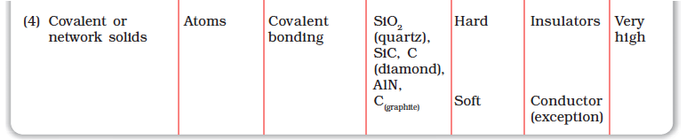
A wide variety of crystalline solids of non-metals result from the formation of covalent bonds between adjacent atoms throughout the crystal. They are also called giant molecules. Covalent bonds are strong and directional in nature, therefore atoms are held very strongly at their positions. Such solids are very hard and brittle. They have extremely high melting points and may even decompose before melting. They are insulators and do not conduct electricity. Diamond (Fig. 1.3) and silicon carbide are typical examples of such solids. Although Graphite (Fig. 1.4) also belongs to this class of crystals, but it is soft and is a conductor of electricity. Its exceptional properties are due to its typical structure. Carbon atoms are arranged in different layers and each atom is covalently bonded to three of its neighbouring atoms in the same layer. The fourth valence electron of each atom is present between different layers and is free to move about. These free electrons make graphite a good conductor of electricity. Different layers can slide one over the other. This makes graphite a soft solid and a good solid lubricant.
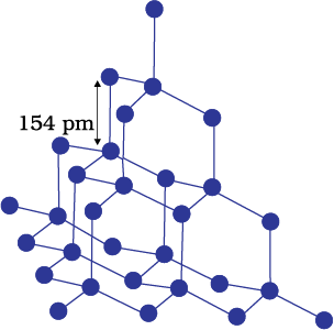
Fig. 1.3: Network structure of diamond
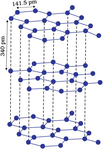
Fig. 1.4: Structure of graphite
The different properties of the four types of solids are listed in Table 1.2.
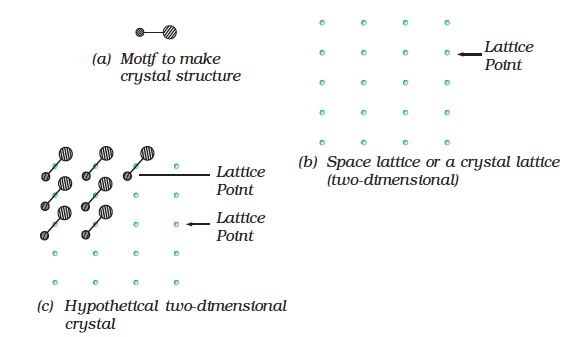
Spacial arrangement of lattice points gives rise to different types of lattices. Fig 1.6 shows arrangement of points in two different lattices.
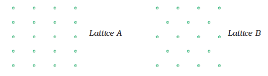
Fig. 1.6: Arrangement of points in two different lattices
In the case of crystalline solids, space lattice is a three-dimensional array of points. The crystal structure is obtained by associating structurral motifs with lattice points. Each repeated basis or motif has same structure and same spacial orientation as other one in a crystal. The environment of each motif is same throughout the crystal except for on surface.
Following are the characteristics of a crystal lattice:
(a) Each point in a lattice is called lattice point or lattice site.
(b) Each point in a crystal lattice represents one constituent particle which may be an atom, a molecule (group of atoms) or an ion.
(c) Lattice points are joined by straight lines to bring out the geometry of the lattice.
We need only a small part of the space lattice of a crystal to spacify crystal completely. This small part is called unit cell. One can choose unit cell in many ways. Normally that cell is chosen which has perpendicular sides of shortest length and one can construct entire crystal by translational displacement of the unit cell in three dimensions. Fig. 1.7 shows movement of unit cell of a two-dimensional lattice to construct the entire crystal structure. Also, unit cells have shapes such that these fill the whole lattice without leaving space between cells.
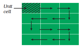
Fig. 1.7:Generating hypothetical two-dimensional crystal structure by shifting square in the direction of arrows.
In two dimensions a parallelogram with side of length ‘a’ and ‘b’ and an angle r between these sides is chosen as unit cell. Possible unit cells in two dimensions are shown in Fig. 1.8.
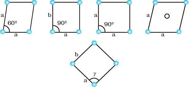
Fig. 1.8: Possible unit cells in two dimensions
A portion of three-dimensional crystal lattice and its unit cell is shown in Fig. 1.9.
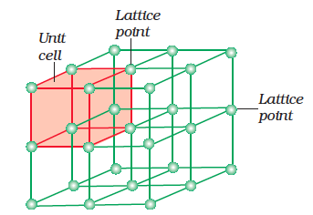
Fig. 1.9: A portion of a threedimensional cubic space of a crystal lattice and its unit cell.
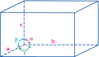
In the three-dimensional crystal structure, unit cell is characterised by:
(i) its dimensions along the three edges a, b and c. These edges may or may not be mutually perpendicular.
(ii) angles between the edges, α (between b and c), β (between a and c) and γ (between a and b). Thus, a unit cell is characterised by six parameters a, b, c, α , β and γ.
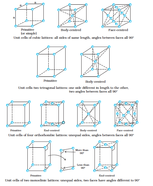
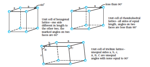
Unit cells can be broadly divided into two categories, primitive and centred unit cells.
(a) Primitive Unit Cells
When constituent particles are present only on the corner positions of a unit cell, it is called as primitive unit cell.
(b) Centred Unit Cells
When a unit cell contains one or more constituent particles present at positions other than corners in addition to those at corners, it is called a centred unit cell. Centred unit cells are of three types:
(i) Body-Centred Unit Cells: Such a unit cell contains one constituent particle (atom, molecule or ion) at its body-centre besides the ones that are at its corners.
(ii) Face-Centred Unit Cells: Such a unit cell contains one constituent particle present at the centre of each face, besides the ones that are at its corners.
(iii) End-Centred Unit Cells: In such a unit cell, one constituent particle is present at the centre of any two opposite faces besides the ones present at its corners.
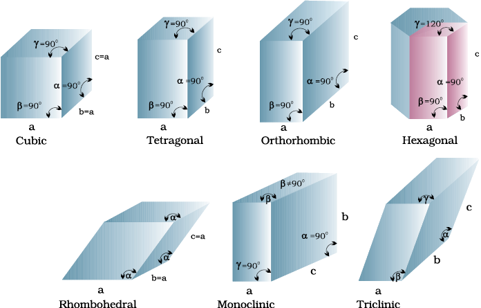
Table 1.3: Seven Primitive Unit Cells and their Possible Variations as Centred Unit Cells
Unit Cells of 14 Types of Bravais Lattices
We know that any crystal lattice is made up of a very large number of unit cells and every lattice point is occupied by one constituent particle (atom, molecule or ion). Let us now work out what portion of each particle belongs to a particular unit cell.
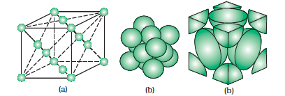
We shall consider three types of cubic unit cells and for simplicity assume that the constituent particle is an atom.
A body-centred cubic (bcc) unit cell has an atom at each of its corners and also one atom at its body centre. Fig. 1.14 depicts (a) open structure (b) space filling model and (c) the unit cell with portions of atoms actually belonging to it. It can be seen that the atom at the body centre wholly belongs to the unit cell in which it is present. Thus in a body-centered cubic (bcc) unit cell:
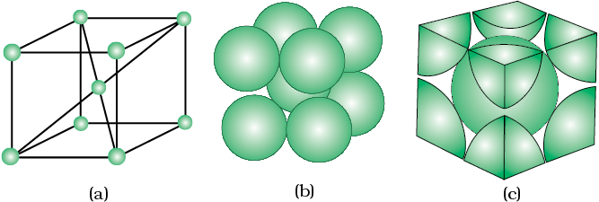
Fig. 1.14: A body-centred cubic unit cell (a) open structure (b) spacefilling structure (c) actual portions of atoms belonging to one unit cell.
(i) 8 corners × per corner atom atom
(ii) 1 body centre atom = 1 × 1 = 1 atom
∴ Total number of atoms per unit cell = 2 atoms
A face-centred cubic (fcc) unit cell contains atoms at all the corners and at the centre of all the faces of the cube. It can be seen in Fig. 1.15 that each atom located at the face-centre is shared between two adjacent unit cells and only of each atom belongs to a unit cell. Fig. 1.16 depicts (a) open structure (b) space-filling model and (c) the unit cell with portions of atoms actually belonging to it. Thus, in a face-centred cubic (fcc) unit cell:
(i) 8 corners atoms × atom per unit cell = 1 atom
(ii) 6 face-centred atoms × atom per unit cell = 6 × = 3 atoms
∴ Total number of atoms per unit cell = 4 atoms
Intext Questions
1.9 Give the significance of a ‘lattice point’.
1.10 Name the parameters that characterise a unit cell.
1.11 Distinguish between
(i) Hexagonal and monoclinic unit cells
(ii) Face-centred and end-centred unit cells.
1.12 Explain how much portion of an atom located at (i) corner and (ii) body-centre of a cubic unit cell is part of its neighbouring unit cell.
In solids, the constituent particles are close-packed, leaving the minimum vacant space. Let us consider the constituent particles as identical hard spheres and build up the three-dimensional structure in three steps.
(a) Close Packing in One Dimension
There is only one way of arranging spheres in a one-dimensional close packed structure, that is to arrange them in a row and touching each other (Fig. 1.17).

Fig. 1.17: Close packing of spheres in one dimension
In this arrangement, each sphere is in contact with two of its neighbours. The number of nearest neighbours of a particle is called its coordination number. Thus, in one dimensional close packed arrangement, the coordination number is 2.
(b) Close Packing in Two Dimensions
Two dimensional close packed structure can be generated by stacking (placing) the rows of close packed spheres. This can be done in two different ways.
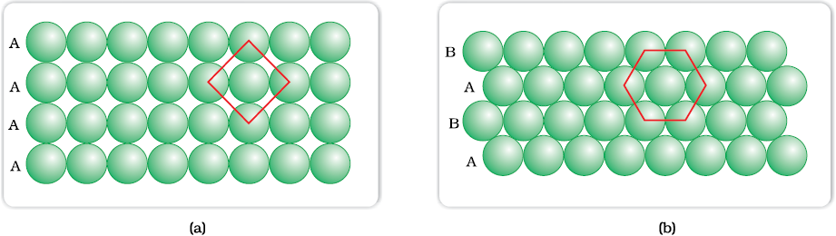
Fig. 1.18: (a) Square close packing (b) hexagonal close packing of spheres in two dimensions
In this arrangement, each sphere is in contact with four of its neighbours. Thus, the two dimensional coordination number is 4. Also, if the centres of these 4 immediate neighbouring spheres are joined, a square is formed. Hence this packing is called square close packing in two dimensions.
(ii) The second row may be placed above the first one in a staggered manner such that its spheres fit in the depressions of the first row. If the arrangement of spheres in the first row is called ‘A’ type, the one in the second row is different and may be called ‘B’ type. When the third row is placed adjacent to the second in staggered manner, its spheres are aligned with those of the first layer. Hence this layer is also of ‘A’ type. The spheres of similarly placed fourth row will be aligned with those of the second row (‘B’ type). Hence this arrangement is of ABAB type. In this arrangement there is less free space and this packing is more efficient than the square close packing. Each sphere is in contact with six of its neighbours and the two dimensional coordination number is 6. The centres of these six spheres are at the corners of a regular hexagon (Fig. 1.18 b) hence this packing is called two dimensional hexagonal close-packing. It can be seen in Figure 1.18 (b) that in this layer there are some voids (empty spaces). These are triangular in shape. The triangular voids are of two different types. In one row, the apex of the triangles are pointing upwards and in the next layer downwards.
(c) Close Packing in Three Dimensions
All real structures are three dimensional structures. They can be obtained by stacking two dimensional layers one above the other. In the last Section, we discussed close packing in two dimensions which can be of two types; square close-packed and hexagonal close-packed. Let us see what types of three dimensional close packing can be obtained from these.
(i) Three-dimensional close packing forms two-dimensional square close-packed layers: While placing the second square close-packed layer above the first we follow the same rule that was followed when one row was placed adjacent to the other. The second layer is placed over the first layer such that the spheres of the upper layer are exactly above those of the first layer. In this arrangement spheres of both the layers are perfectly aligned horizontally as well as vertically as shown in Fig. 1.19. Similarly, we may place more layers one above the other. If the arrangement of spheres in the first layer is called ‘A’ type, all the layers have the same arrangement. Thus this lattice has AAA.... type pattern. The lattice thus generated is the simple cubic lattice, and its unit cell is the primitive cubic unit cell (See Fig. 1.19).
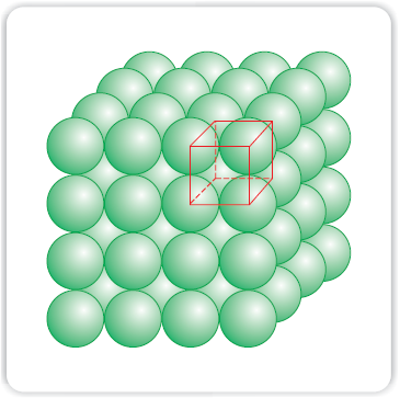
Fig. 1.19: Simple cubic lattice formed by A A A .... arrangement
(ii) Three dimensional close packing from two dimensional hexagonal close packed layers: Three dimensional close packed structure can be generated by placing layers one over the other.
(a) Placing second layer over the first layer
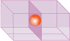
Let us take a two dimensional hexagonal close packed layer ‘A’ and place a similar layer above it such that the spheres of the second layer are placed in the depressions of the first layer. Since the spheres of the two layers are aligned differently, let us call the second layer as B. It can be observed from Fig. 1.20 that all the triangular voids of the first layer are not covered by the spheres of the second layer. This gives rise to different arrangements. Wherever a sphere of the second layer is above the void of the first layer (or vice versa) a tetrahedral void is formed. These voids are called tetrahedral voids because a tetrahedron is formed when the centres of these four spheres are joined. Theyhave been marked as ‘T’ in Fig. 1.20. One such void has been shown separately in Fig. 1.21.
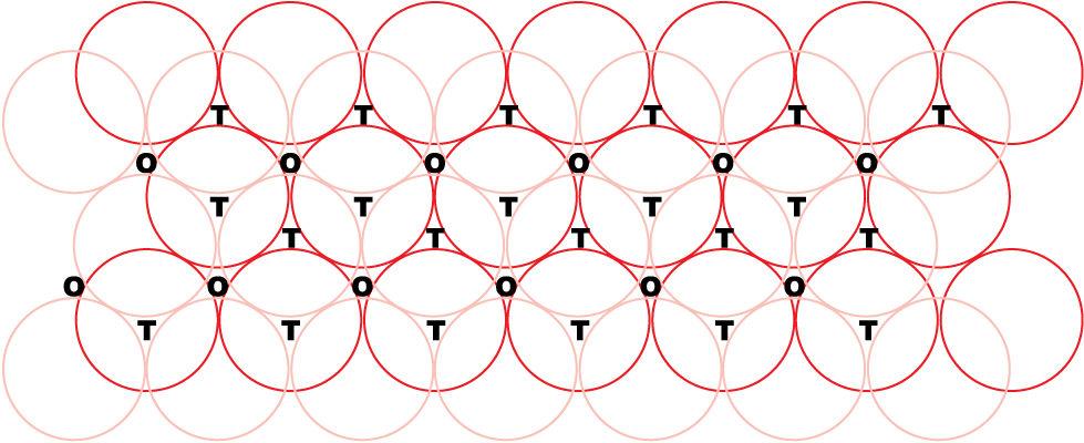
Fig. 1.16: A stack of two layers of close packed spheres and voids generated in them. T = Tetrahedral void; O = Octahedral void
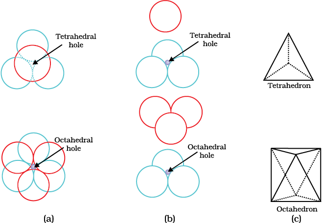
Fig 1.17 Tetrahedral and octahedral voids (a) top view (b) exploded side view and (c) geometrical shape of the void.
Let the number of close packed spheres be N, then:
The number of octahedral voids generated = N
The number of tetrahedral voids generated = 2N
(b) Placing third layer over the second layer
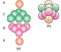
(i) Covering Tetrahedral Voids: Tetrahedral voids of the second layer may be covered by the spheres of the third layer. In this case, the spheres of the third layer are exactly aligned with those of the first layer. Thus, the pattern of spheres is repeated in alternate layers. This pattern is often written as ABAB ....... pattern. This structure is called hexagonal close packed (hcp) structure (Fig. 1.22). This sort of arrangement of atoms is found in many metals like magnesium and zinc.
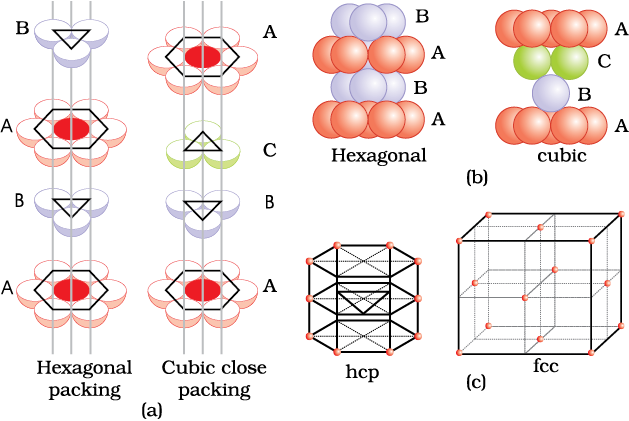
(ii) Covering Octahedral Voids: The third layer may be placed above the second layer in a manner such that its spheres cover the octahedral voids. When placed in this manner, the spheres of the third layer are not aligned with those of either the first or the second layer. This arrangement is called ‘C’ type. Only when fourth layer is placed, its spheres are aligned with those of the first layer as shown in Figs. 1.22 and 1.23. This pattern of layers is often written as ABCABC ........... This structure is called cubic close packed (ccp) or face-centred cubic (fcc) structure. Metals such as copper and silver crystallise in this structure.
Both these types of close packing are highly efficient and 74% space in the crystal is filled. In either of them, each sphere is in contact with twelve spheres. Thus, the coordination number is 12 in either of these two structures.
Earlier in the section, we have learnt that when particles are close-packed resulting in either ccp or hcp structure, two types of voids are generated. While the number of octahedral voids present in a lattice is equal to the number of close packed particles, the number of tetrahedral voids generated is twice this number. In ionic solids, the bigger ions (usually anions) form the close packed structure and the smaller ions (usually cations) occupy the voids. If the latter ion is small enough then tetrahedral voids are occupied, if bigger, then octahedral voids. All octahedral or tetrahedral voids are not occupied. In a given compound, the fraction of octahedral or tetrahedral voids that are occupied, depends upon the chemical formula of the compound, as can be seen from the following examples.
Example 1.1
A compound is formed by two elements X and Y. Atoms of the element Y (as anions) make ccp and those of the element X (as cations) occupy all the octahedral voids. What is the formula of the compound?
Solution
The ccp lattice is formed by the element Y. The number of octahedral voids generated would be equal to the number of atoms of Y present in it. Since all the octahedral voids are occupied by the atoms of X, their number would also be equal to that of the element Y. Thus, the atoms of elements X and Y are present in equal numbers or 1:1 ratio. Therefore, the formula of the compound is XY.
Example 1.2
Atoms of element B form hcp lattice and those of the element A occupy 2/3rd of tetrahedral voids. What is the formula of the compound formed by the elements A and B?
Solution
The number of tetrahedral voids formed is equal to twice the number of atoms of element B and only 2/3rd of these are occupied by the atoms of element A. Hence the ratio of the number of atoms of A and B is 2 × (2/3):1 or 4:3 and the formula of the compound is A4B3.
Locating Tetrahedral and Octahedral Voids
We know that close packed structures have both tetrahedral and octahedral voids. Let us take ccp (or fcc) structure and locate these voids in it.
(a) Locating Tetrahedral Voids
Let us consider a unit cell of ccp or fcc lattice [Fig. 1(a)]. The unit cell is divided into eight small cubes.
Each small cube has atoms at alternate corners [Fig. 1(a)]. In all, each small cube has 4 atoms. When joined to each other, they make a regular tetrahedron. Thus, there is one tetrahedral void in each small cube and eight tetrahedral voids in total. Each of the eight small cubes have one void in one unit cell of ccp structure. We know that ccp structure has 4 atoms per unit cell. Thus, the number of tetrahedral voids is twice the number of atoms.
(b) Locating Octahedral Voids
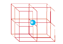
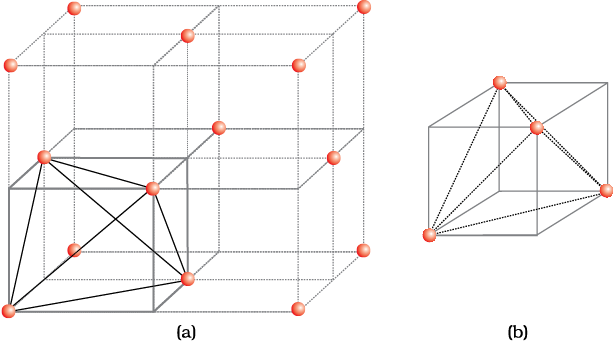
Let us again consider a unit cell of ccp or fcc lattice [Fig. 2(a)]. The body centre of the cube, C is not occupied but it is surrounded by six atoms on face centres. If these face centres are joined, an octahedron is generated. Thus, this unit cell has one octahedral void at the body centre of the cube.
Besides the body centre, there is one octahedral void at the centre of each of the 12 edges [Fig. 2(b)]. It is surrounded by six atoms, four belonging to the same unit cell (2 on the corners and 2 on face centre) and two belonging to two adjacent unit cells. Since each edge of the cube is shared between four adjacent unit cells, so is the octahedral void located on it. Only th of each void belongs to a particular unit cell.
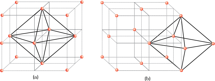
Fig. 2: Location of octahedral voids per unit cell of ccp or fcc lattice (a) at the body centre of the cube and (b) at the centre of each edge (only one such void is shown).
Thus in cubic close packed structure:
Octahedral void at the body-centre of the cube = 1
12 octahedral voids located at each edge and shared between four unit cells
=
∴ Total number of octahedral voids = 4
We know that in ccp structure, each unit cell has 4 atoms. Thus, the number of octahedral voids is equal to this number.
In whatever way the constituent particles (atoms, molecules or ions) are packed, there is always some free space in the form of voids. Packing efficiency is the percentage of total space filled by the particles. Let us calculate the packing efficiency in different types of structures.
Both types of close packing (hcp and ccp) are equally efficient. Let us calculate the efficiency of packing in ccp structure. In Fig. 1.24 let the unit cell edge length be ‘a’ and face diagonal AC = b.
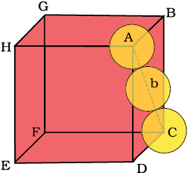
Fig. 1.24: Cubic close packing other sides are not provided with spheres for sake of clarity.
In 
AC2 = b2 = BC2 + AB2
= a2+a2 = 2a2 or
b = 
If r is the radius of the sphere, we find
b = 4r =
or a = 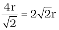
(we can also write, 
We know, that each unit cell in ccp structure, has effectively 4 spheres. Total volume of four spheres is equal to 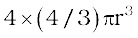 and volume of the cube is a3 or
  .
.
Therefore,

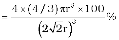
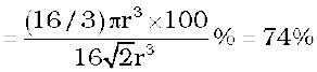
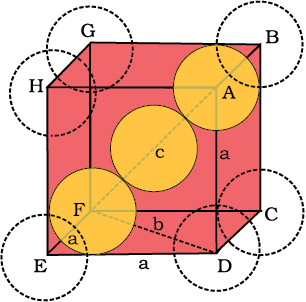
Fig. 1.25: Body-centred cubic unit cell (sphere along the body diagonal are shown with solid boundaries).
From Fig. 1.25, it is clear that the atom at the centre will be in touch with the other two atoms diagonally arranged.
In ∆ EFD,
b2 = a2 + a2 = 2a2
b =
Now in ∆ AFD
c2 = a2 + b2 = a2 + 2a2 = 3a2
c =
The length of the body diagonal c is equal to 4r, where r is the radius of the sphere (atom), as all the three spheres along the diagonal touch each other.
Therefore, = 4r
a =
Also we can write, r = a
In this type of structure, total number of atoms is 2 and their volume is
Volume of the cube, a3 will be equal to or
Therefore,
In a simple cubic lattice the atoms are located only on the corners of the cube. The particles touch each other along the edge (Fig. 1.26).
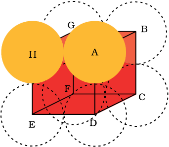
Fig. 1.26 Simple cubic unit cell. The spheres are in contact with each other along the edge of the cube.
Thus, the edge length or side of the cube ‘a’, and the radius of each particle, r are related as
a = 2r
The volume of the cubic unit cell = a3 = (2r)3 = 8r3
Since a simple cubic unit cell contains only 1 atom
The volume of the occupied space =
∴ Packing efficiency
=
=
= 52.36% = 52.4 %
Thus, we may conclude that ccp and hcp structures have maximum packing efficiency.
From the unit cell dimensions, it is possible to calculate the volume of the unit cell. Knowing the density of the metal, we can calculate the mass of the atoms in the unit cell. The determination of the mass of a single atom gives an accurate method of determination of Avogadro constant. Suppose, edge length of a unit cell of a cubic crystal determined by X-ray diffraction is a, d the density of the solid substance and M the molar mass. In case of cubic crystal:
Volume of a unit cell = a3
Mass of the unit cell
= number of atoms in unit cell × mass of each atom = z × m
(Here z is the number of atoms present in one unit cell and m is the mass of a single atom)
Mass of an atom present in the unit cell:
m (M is molar mass)
Therefore, density of the unit cell
Remember, the density of the unit cell is the same as the density of the substance. The density of the solid can always be determined by other methods. Out of the five parameters (d, z, M, a and NA), if any four are known, we can determine the fifth.
Example 1.3
An element has a body-centred cubic (bcc) structure with a cell edge of 288 pm. The density of the element is 7.2 g/cm3. How many atoms are present in 208 g of the element?
Solution
Volume of the unit cell = (288 pm)3
= (288×10-12 m)3 = (288×10-10 cm)3
= 2.39×10⁻²³ cm3
Volume of 208 g of the element
Number of unit cells in this volume
= 12.08×10²³ unit cells
Since each bcc cubic unit cell contains 2 atoms, therefore, the total number of atoms in 208 g = 2 (atoms/unit cell) × 12.08 × 10²³ unit cells
= 24.16×10²³ atoms
Example 1.4
X-ray diffraction studies show that copper crystallises in an fcc unit cell with cell edge of 3.608×10⁻⁸ cm. In a separate experiment, copper is determined to have a density of 8.92 g/cm3, calculate the atomic mass of copper.
Solution
In case of fcc lattice, number of atoms per unit cell, z = 4 atoms
Therefore, M =
= 63.1 g/mol
Atomic mass of copper = 63.1u
Example 1.5
Silver forms ccp lattice and X-ray studies of its crystals show that the edge length of its unit cell is 408.6 pm. Calculate the density of silver (Atomic mass = 107.9 u).
Solution
Since the lattice is ccp, the number of silver atoms per unit cell = z = 4
Molar mass of silver = 107.9 g mol–1 = 107.9×10⁻³ kg mol–1
Edge length of unit cell = a = 408.6 pm = 408.6×10⁻¹² m
Density, d =
= = 10.5×10³ kg m–3
= 10.5 g cm-3
Intext Questions
1.13 What is the two dimensional coordination number of a molecule in square close-packed layer?
1.14 A compound forms hexagonal close-packed structure. What is the total number of voids in 0.5 mol of it? How many of these are tetrahedral voids?
1.15 A compound is formed by two elements M and N. The element N forms ccp and atoms of M occupy 1/3rd of tetrahedral voids. What is the formula of the compound?
1.16 Which of the following lattices has the highest packing efficiency (i) simple cubic (ii) body-centred cubic and (iii) hexagonal close-packed lattice?
1.17 An element with molar mass 2.7×10⁻² kg mol-1 forms a cubic unit cell with edge length 405 pm. If its density is 2.7×10³ kg m-3, what is the nature of the cubic unit cell?
(a) Stoichiometric Defects
These are the point defects that do not disturb the stoichiometry of the solid. They are also called intrinsic or thermodynamic defects. Basically these are of two types, vacancy defects and interstitial defects.
(i) Vacancy Defect: When some of the lattice sites are vacant, the crystal is said to have vacancy defect (Fig. 1.27). This results in decrease in density of the substance. This defect can also develop when a substance is heated.
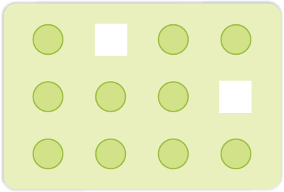
Fig. 1.27: Vacancy defects
(ii) Interstitial Defect: When some constituent particles (atoms or molecules) occupy an interstitial site, the crystal is said to have interstitial defect (Fig. 1.28). This defect increases the density of the substance.
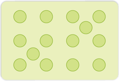
Fig. 1.28: Interstitial defects
(iii) Frenkel Defect: This defect is shown by ionic solids. The smaller ion (usually cation) is dislocated from its normal site to an interstitial site (Fig. 1.29). It creates avacancy defect at its original site and an interstitial defect at its new location.
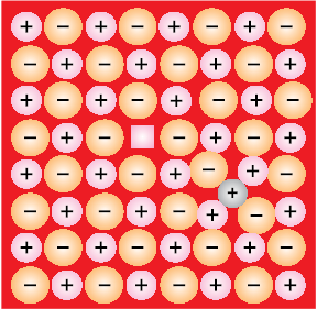
Fig. 1.29: Frenkel defects
Frenkel defect is also called dislocation defect. It does not change the density of the solid. Frenkel defect is shown by ionic substance in which there is a large difference in the size of ions, for example, ZnS, AgCl, AgBr and AgI due to small size of Zn2+ and Ag+ ions.
(iv) Schottky Defect: It is basically a vacancy defect in ionic solids. In order to maintain electrical neutrality, the number of missing cations and anions are equal (Fig. 1.30).
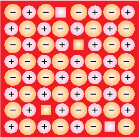
Fig. 1.30: Schottky defects
(b) Impurity Defects
If molten NaCl containing a little amount of SrCl2 is crystallised, some of the sites of Na+ ions are occupied by Sr2+ (Fig.1.31). Each Sr2+ replaces two Na+ ions. It occupies the site of one ion and the other site remains vacant. The cationic vacancies thus produced are equal in number to that of Sr2+ ions. Another similar example is the solid solution of CdCl2 and AgCl.
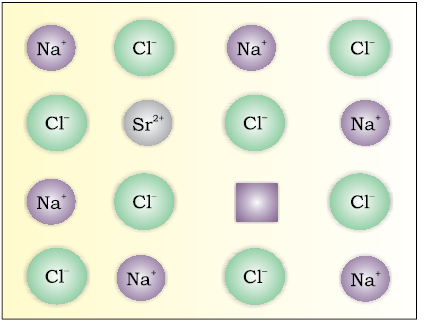
Fig. 1.31: Introduction of cation vacancy in NaCl by substitution of Na+ by Sr2+
(c) Non-Stoichiometric Defects
The defects discussed so far do not disturb the stoichiometry of the crystalline substance. However, a large number of non-stoichiometric inorganic solids are known which contain the constituent elements in non-stoichiometric ratio due to defects in their crystal structures. These defects are of two types: (i) metal excess defect and (ii) metal deficiency defect.
(i) Metal Excess Defect
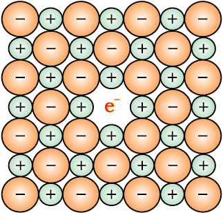
Fig. 1.32: An F-centre in a crystal
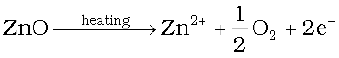
Now there is excess of zinc in the crystal and its formula becomes Zn1+xO. The excess Zn2+ ions move to interstitial sites and the electrons to neighbouring interstitial sites.
(ii) Metal Deficiency Defect
There are many solids which are difficult to prepare in the stoichiometric composition and contain less amount of the metal as compared to the stoichiometric proportion. A typical example of this type is FeO which is mostly found with a composition of Fe0.95O. It may actually range from Fe0.93O to Fe0.96O. In crystals of FeO some Fe2+ cations are missing and the loss of positive charge is made up by the presence of required number of Fe3+ ions.
Solids exhibit an amazing range of electrical conductivities, extending over 27 orders of magnitude ranging from 10–20 to 107 ohm–1 m–1. Solids can be classified into three types on the basis of their conductivities.
(i) Conductors: The solids with conductivities ranging between 104 to 107 ohm–1m–1 are called conductors. Metals have conductivities in the order of 107 ohm–1m–1 are good conductors.
(ii) Insulators : These are the solids with very low conductivities ranging between 10–20 to 10–10 ohm–1m–1.
(iii) Semiconductors : These are the solids with conductivities in the intermediate range from 10–6 to 104 ohm–1m–1.
A conductor may conduct electricity through movement of electrons or ions. Metallic conductors belong to the former category and electrolytes to the latter.
Metals conduct electricity in solid as well as molten state. The conductivity of metals depend upon the number of valence electrons available per atom. The atomic orbitals of metal atoms form molecular orbitals which are so close in energy to each other as to form a band. If this band is partially filled or it overlaps with a higher energy unoccupied conduction band, then electrons can flow easily under an applied electric field and the metal shows conductivity (Fig. 1.33 a).
If the gap between filled valence band and the next higher unoccupied band (conduction band) is large, electrons cannot jump to it and such a substance has very small conductivity and it behaves as an insulator (Fig. 1.33 b).
In case of semiconductors, the gap between the valence band and conduction band is small (Fig. 1.33 c). Therefore, some electrons may jump to conduction band and show some conductivity. Electrical conductivity of semiconductors increases with rise in temperature, since more electrons can jump to the conduction band. Substances like silicon and germanium show this type of behaviour and are called intrinsic semiconductors.
The conductivity of these intrinsic semiconductors is too low to be of practical use. Their conductivity is increased by adding an appropriate amount of suitable impurity. This process is called doping. Doping can be done with an impurity which is electron rich or electron deficient as compared to the intrinsic semiconductor silicon or germanium. Such impurities introduce electronic defects in them.
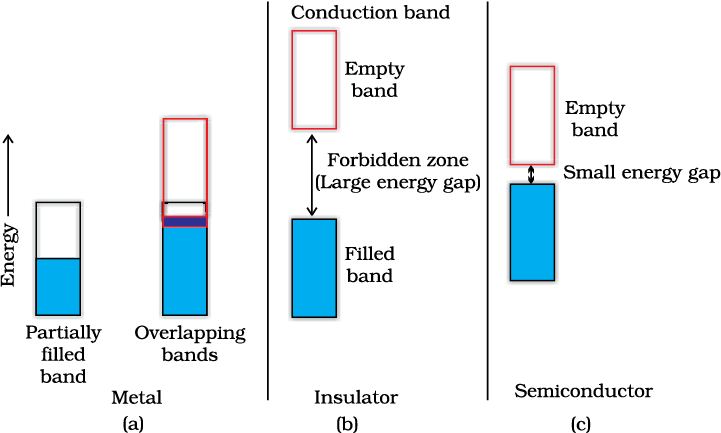
Fig. 1.33 Distinction among (a) metals (b) insulators and (c) semiconductors. In each case, an unshaded area represents a conduction band.
(a) Electron – rich impurities
Silicon and germanium belong to group 14 of the periodic table and have four valence electrons each. In their crystals each atom forms four covalent bonds with its neighbours (Fig. 1.34 a). When doped with a group 15 element like P or As, which contains five valence electrons, they occupy some of the lattice sites in silicon or germanium crystal (Fig. 1.34 b). Four out of five electrons are used in the formation of four covalent bonds with the four neighbouring silicon atoms. The fifth electron is extra and becomes delocalised. These delocalised electrons increase the conductivity of doped silicon (or germanium). Here the increase in conductivity is due to the negatively charged electron, hence silicon doped with electron-rich impurity is called n-type semiconductor.
(b) Electron – deficit impurities
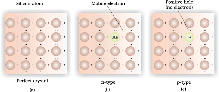
Fig. 1.34: Creation of n-type and p-type semiconductors by doping groups 13 and 15 elements.
Applications of n-type and p-type semiconductors
Various combinations of n-type and p-type semiconductors are used for making electronic components. Diode is a combination of n-type and p-type semiconductors and is used as a rectifier. Transistors are made by sandwiching a layer of one type of semiconductor between two layers of the other type of semiconductor. npn and pnp type of transistors are used to detect or amplify radio or audio signals. The solar cell is an efficient photo-diode used for conversion of light energy into electrical energy.
Germanium and silicon are group 14 elements and therefore, have a characteristic valence of four and form four bonds as in diamond. A large variety of solid state materials have been prepared by combination of groups 13 and 15 or 12 and 16 to simulate average valence of four as in Ge or Si. Typical compounds of groups 13 – 15 are InSb, AlP and GaAs. Gallium arsenide (GaAs) semiconductors have very fast response and have revolutionised the design of semiconductor devices. ZnS, CdS, CdSe and HgTe are examples of groups 12 – 16 compounds. In these compounds, the bonds are not perfectly covalent and the ionic character depends on the electronegativities of the two elements.
It is interesting to learn that transition metal oxides show marked differences in electrical properties. TiO, CrO2 and ReO3 behave like metals. Rhenium oxide, ReO3 is like metallic copper in its conductivity and appearance. Certain other oxides like VO, VO2, VO3 and TiO3 show metallic or insulating properties depending on temperature.
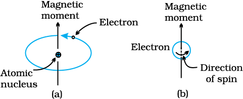
(i) Paramagnetism: Paramagnetic substances are weakly attracted by a magnetic field. They are magnetised in a magnetic field in the same direction. They lose their magnetism in the absence of magnetic field. Paramagnetism is due to presence of one or more unpaired electrons which are attracted by the magnetic field. O2, Cu2+, Fe3+, Cr3+ are some examples of such substances.
(ii) Diamagnetism: Diamagnetic substances are weakly repelled by a magnetic field. H2O, NaCl and C6H6 are some examples of such substances. They are weakly magnetised in a magnetic field in opposite direction. Diamagnetism is shown by those substances in which all the electrons are paired and there are no unpaired electrons. Pairing of electrons cancels their magnetic moments and they lose their magnetic character.
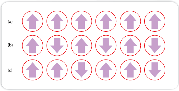
(iii) Ferromagnetism: A few substances like iron, cobalt, nickel, gadolinium and CrO2 are attracted very strongly by a magnetic field. Such substances are called ferromagnetic substances. Besides strong attractions, these substances can be permanently magnetised. In solid state, the metal ions of ferromagnetic substances are grouped together into small regions called domains. Thus, each domain acts as a tiny magnet. In an unmagnetised piece of a ferromagnetic substance the domains are randomly oriented and their magnetic moments get cancelled. When the substance is placed in a magnetic field all the domains get oriented in the direction of the magnetic field (Fig. 1.36 a) and a strong magnetic effect is produced. This ordering of domains persist even when the magnetic field is removed and the ferromagnetic substance becomes a permanent magnet.
(iv) Antiferromagnetism: Substances like MnO showing anti-ferromagnetism have domain structure similar to ferromagnetic substance, but their domains are oppositely oriented and cancel out each other’s magnetic moment (Fig. 1.36 b).
(v) Ferrimagnetism: Ferrimagnetism is observed when the magnetic moments of the domains in the substance are aligned in parallel and anti-parallel directions in unequal numbers (Fig. 1.36c). They are weakly attracted by magnetic field as compared to ferromagnetic substances. Fe3O4 (magnetite) and ferrites like MgFe2O4 and ZnFe2O4 are examples of such substances. These substances also lose ferrimagnetism on heating and become paramagnetic.
Intext Questions
1.18 What type of defect can arise when a solid is heated? Which physical property is affected by it and in what way?
1.19 What type of stoichiometric defect is shown by:
(i) ZnS (ii) AgBr
1.20 Explain how vacancies are introduced in an ionic solid when a cation of higher valence is added as an impurity in it.
1.21 Ionic solids, which have anionic vacancies due to metal excess defect, develop colour. Explain with the help of a suitable example.
1.22 A group 14 element is to be converted into n-type semiconductor by doping it with a suitable impurity. To which group should this impurity belong?
1.23 What type of substances would make better permanent magnets, ferromagnetic or ferrimagnetic. Justify your answer.
Solids have definite mass, volume and shape. This is due to the fixed position of their constituent particles, short distances and strong interactions between them. In amorphous solids, the arrangement of constituent particles has only short range order and consequently they behave like super cooled liquids, do not have sharp melting points and are isotropic in nature. In crystalline solids there is long range order in the arrangement of their constituent particles. They have sharp melting points, are anisotropic in nature and their particles have characteristic shapes. Properties of crystalline solids depend upon the nature of interactions between their constituent particles. On this basis, they can be divided into four categories, namely: molecular, ionic, metallic and covalent solids. They differ widely in their properties.
The constituent particles in crystalline solids are arranged in a regular pattern which extends throughout the crystal. This arrangement is often depicted in the form of a three dimensional array of points which is called crystal lattice. Each lattice point gives the location of one particle in space. In all, fourteen different types of lattices are possible which are called Bravais lattices. Each lattice can be generated by repeating its small characteristic portion called unit cell. A unit cell is characterised by its edge lengths and three angles between these edges. Unit cells can be either primitive which have particles only at their corner positions or centred. The centred unit cells have additional particles at their body centre (body-centred), at the centre of each face (face-centred) or at the centre of two opposite faces (end-centred). There are seven types of primitive unit cells. Taking centred unit cells also into account, there are fourteen types of unit cells in all, which result in fourteen Bravais lattices.
Close-packing of particles result in two highly efficient lattices, hexagonal close-packed (hcp) and cubic close-packed (ccp). The latter is also called face-centred cubic (fcc) lattice. In both of these packings 74% space is filled. The remaining space is present in the form of two types of voids-octahedral voids and tetrahedral voids. Other types of packing are not close-packings and have less efficient packing of particles. While in body-centred cubic lattice (bcc) 68% space is filled, in simple cubic lattice only 52.4 % space is filled.
Solids are not perfect in structure. There are different types of imperfections or defects in them. Point defects and line defects are common types of defects. Point defects are of three types - stoichiometric defects, impurity defects and non-stoichiometric defects. Vacancy defects and interstitial defects are the two basic types of stoichiometric point defects. In ionic solids, these defects are present as Frenkel and Schottky defects. Impurity defects are caused by the presence of an impurity in the crystal. In ionic solids, when the ionic impurity has a different valence than the main compound, some vacancies are created. Non-stoichiometric defects are of metal excess type and metal deficient type. Sometimes calculated amounts of impurities are introduced by doping in semiconductors that change their electrical properties. Such materials are widely used in electronics industry. Solids show many types of magnetic properties like paramagnetism, diamagnetism, ferromagnetism, antiferromagnetism and ferrimagnetism. These properties are used in audio, video and other recording devices. All these properties can be correlated with their electronic configurations or structures.
1.1 Define the term ‘amorphous’. Give a few examples of amorphous solids.
NEETprep Answer
1.2 What makes a glass different from a solid such as quartz? Under what conditions could quartz be converted into glass?
NEETprep Answer
1.3 Classify each of the following solids as ionic, metallic, molecular, network (covalent) or amorphous.
(i) Tetra phosphorus decoxide (P4O10) (vii) Graphite
(ii) Ammonium phosphate (NH4)3PO4 (viii) Brass
(iii) SiC (ix) Rb
(iv) I2 (x) LiBr
(v) P4 (xi) Si
(vi) Plastic
NEETprep Answer
1.4 (i) What is meant by the term ‘coordination number’?
(ii) What is the coordination number of atoms:
(a) in a cubic close-packed structure?
(b) in a body-centred cubic structure?
NEETprep Answer
1.5 How can you determine the atomic mass of an unknown metal if you know its density and the dimension of its unit cell? Explain.
NEETprep Answer
1.6 ‘Stability of a crystal is reflected in the magnitude of its melting points’. Comment. Collect melting points of solid water, ethyl alcohol, diethyl ether and methane from a data book. What can you say about the intermolecular forces between these molecules?
NEETprep Answer
1.7 How will you distinguish between the following pairs of terms:
(i) Hexagonal close-packing and cubic close-packing?
(ii) Crystal lattice and unit cell?
(iii) Tetrahedral void and octahedral void?
NEETprep Answer
1.8 How many lattice points are there in one unit cell of each of the following lattice?
(i) Face-centred cubic
(ii) Face-centred tetragonal
(iii) Body-centred
NEETprep Answer
1.9 Explain
(i) The basis of similarities and differences between metallic and ionic crystals.
(ii) Ionic solids are hard and brittle.
1.10 Calculate the efficiency of packing in case of a metal crystal for
(i) Simple cubic
(ii) Body-centred cubic
(iii) Face-centred cubic (with the assumptions that atoms are touching each other).
NEETprep Answer1.11 Silver crystallises in fcc lattice. If edge length of the cell is 4.07 × 10⁻⁸ cm and density is 10.5 g cm−3, calculate the atomic mass of silver.
NEETprep Answer1.12 A cubic solid is made of two elements P and Q. Atoms of Q are at the corners of the cube and P at the body-centre. What is the formula of the compound? What are the coordination numbers of P and Q?
NEETprep Answer1.13 Niobium crystallises in body-centred cubic structure. If density is 8.55 g cm−3, calculate atomic radius of niobium using its atomic mass 93 u.
NEETprep Answer1.14 If the radius of the octahedral void is r and radius of the atoms in close packing is R, derive a relation between r and R.
NEETprep Answer1.15 Copper crystallises into a fcc lattice with edge length 3.61 × 10⁻⁸ cm. Show that the calculated density is in agreement with its measured value of 8.92 g cm−3.
NEETprep Answer1.16 Analysis shows that nickel oxide has the formula Ni0.98O1.00. What fractions of nickel exist as Ni2+ and Ni3+ ions?
NEETprep Answer1.17 What is a semiconductor? Describe the two main types of semiconductors and contrast their conduction mechanism.
NEETprep Answer1.18 Non-stoichiometric cuprous oxide, Cu2O can be prepared in laboratory. In this oxide, copper to oxygen ratio is slightly less than 2:1. Can you account for the fact that this substance is a p-type semiconductor?
NEETprep Answer1.19 Ferric oxide crystallises in a hexagonal close-packed array of oxide ions with two out of every three octahedral holes occupied by ferric ions. Derive the formula of the ferric oxide.
NEETprep Answer1.20 Classify each of the following as being either a p-type or an n-type semiconductor:
(i) Ge doped with In (ii) B doped with Si.
21. Gold (atomic radius = 0.144 nm) crystallises in a face-centred unit cell. What is the length of a side of the cell?
NEETprep Answer22. In terms of band theory, what is the difference
(i) Between a conductor and an insulator
(ii) Between a conductor and a semiconductor
NEETprep Answer23. Explain the following terms with suitable examples:
(i) Schottky defect
(ii) Frenkel defect
(iii) Interstitials and
(iv) F-centres
NEETprep Answer24. Aluminium crystallises in a cubic close-packed structure. Its metallic radius is 125 pm.
(i) What is the length of the side of the unit cell?
(ii) How many unit cells are there in 1.00 cm3 of aluminium?
NEETprep Answer25. If NaCl is doped with 10−3 mol % of SrCl2, what is the concentration of cation vacancies?
NEETprep Answer26. Explain the following with suitable examples:
(i) Ferromagnetism
(ii)Paramagnetism
(iii)Ferrimagnetism
(iv)Antiferromagnetism
(v)12-16 and 13-15 group compounds.
NEETprep AnswerINTEXT QUESTIONS
1.1 Why are solids rigid?
NEETprep Answer1.2 Why do solids have a definite volume?
NEETprep Answer1.3 Classify the following as amorphous or crystalline solids:
Polyurethane, naphthalene, benzoic acid, Teflon, potassium nitrate, cellophane, polyvinyl chloride, fibreglass, copper.
NEETprep Answer1.4 Why is glass considered a supercooled liquid?
NEETprep Answer1.6 Classify the following solids in different categories based on the nature of intermolecular forces operating in them:
Potassium sulphate, tin, benzene, urea, ammonia, water, zinc sulphide, graphite, rubidium, argon, silicon carbide.
NEETprep Answer1.7 Solid A is a very hard electrical insulator in solid as well as in molten state and melts at extremely high temperature. What type of solid is it?
NEETprep Answer1.8 Ionic solids conduct electricity in molten state but not in solid state. Explain.
NEETprep Answer1.9 What type of solids are electrical conductors, malleable and ductile?
NEETprep Answer1.10 Give the significance of a ‘lattice point’.
NEETprep Answer1.11 Name the parameters that characterize a unit cell.
NEETprep Answer1.12 Distinguish between
(i) Hexagonal and monoclinic unit cells
(ii) Face-centred and end-centred unit cells.
NEETprep Answer1.13 Explain how much portion of an atom located at (i) corner and (ii) body centre of a cubic unit cell is part of its neighbouring unit cell.
NEETprep Answer1.14 What is the two dimensional coordination number of a molecule in square close packed layer?
NEETprep Answer1.15 A compound forms hexagonal close-packed structure. What is the total number of voids in 0.5 mol of it? How many of these are tetrahedral voids?
NEETprep Answer1.16 A compound is formed by two elements M and N. The element N forms ccp and atoms of M occupy 1/3rd of tetrahedral voids. What is the formula of the compound?
NEETprep Answer1.17 Which of the following lattices has the highest packing efficiency (i) simple cubic (ii) body-centred cubic and (iii) hexagonal close-packed lattice?
NEETprep Answer1.18 An element with molar mass 2.7 × 10⁻² kg mol-1 forms a cubic unit cell with edge length 405 pm. If its density is 2.7 × 10³ kg m−3, what is the nature of the cubic unit cell?
NEETprep Answer1.19 What type of defect can arise when a solid is heated? Which physical property is affected by it and in what way?
NEETprep Answer1.20 What type of stoichiometric defect is shown by:
(i) ZnS (ii) AgBr
NEETprep Answer1.21 Explain how vacancies are introduced in an ionic solid when a cation of higher valence is added as an impurity in it.
NEETprep Answer1.22 Ionic solids, which have anionic vacancies due to metal excess defect, develop colour. Explain with the help of a suitable example.
NEETprep Answer1.23 A group 14 element is to be converted into n-type semiconductor by doping it with a suitable impurity. To which group should this impurity belong?
NEETprep Answer1.24 What type of substances would make better permanent magnets, ferromagnetic or ferrimagnetic. Justify your answer.
NEETprep Answer
Multiple Choice Questions (MCQs)
1. Which of the following conditions favours the existence of a substance in the solid state?
(a) High temperature
(b) Low temperature
(c) High thermal energy
(d) Weak cohesive forces
NEETprep Answer
2. Which of the following is not a characteristic of a crystalline solid?
(a) Definite and characteristic heat of fusion
(b) Isotropic nature
(c) A regular periodically repeated pattern of arrangement of constituent particles in the entire crystal
(d) A true solid
NEETprep Answer
3. Which of the following is an amorphous solid?
(a) Graphite (C)
(b) Quartz glass ( SiO2 )
(c) Chrome alum
(d) Silicon carbide (SiC)
NEETprep Answer
4. Which of the following arrangements shows schematic alignment of magnetic moments of antiferromagnetic substances?
(a)
(b)
(c)
(d)
NEETprep Answer
5. Which of the following is true about the value of refractive index of quartz glass?
(a) Same in all directions
(b) Different in different directions
(c) Cannot be measured
(d) Always zero
NEETprep Answer
6. Which of the following statement is not true about amorphous solids?
(a) On heating they may become crystalline at certain temperature
(b) They may become crystalline on keeping for long time
(c) Amorphous solids can be moulded by heating
(d) They are anisotropic in nature
NEETprep Answer
7. The sharp melting point of crystalline solids is due to......... .
(a) a regular arrangement of constituent particles observed over a short distance in the crystal lattice
(b) a regular arrangement of constituent particles observed over a long distance in the crystal lattice
(c) same arrangement of constituent particles in different directions
(d) different arrangement of constituent particles in different directions
NEETprep Answer
8. Iodine molecules are held in the crystals lattice by ........ .
(a) London forces
(b) dipole-dipole interactions
(c) covalent bonds
(d) coulombic forces
NEETprep Answer
9. Which of the following is a network solid?
(a) SO2 (solid)
(b) I2
(c) Diamond
(d) H2O (ice)
NEETprep Answer
10. Which of the following solids is not an electrical conductor?
1. Mg(s)
2. TiO (s)
3. I2 (s)
4. H2O (s)
(a) Only 1
(b) Only 2
(c) 3 and 4
(d) 2, 3 and 4
NEETprep Answer
11. Which of the following is not the characteristic of ionic solids?
(a) Very low value of electrical conductivity in the molten state
(b) Brittle nature
(c) Very strong forces of interactions
(d) Anisotropic nature
NEETprep Answer
12. Graphite is a good conductor of electricity due to the presence of ......... .
(a) lone pair of electrons
(b) free valence electrons
(c) cations
(d) anions
NEETprep Answer
13. Which of the following oxides behaves as conductor or insulator depending upon temperature?
(a) TiO
(b) SiO2
(c) TiO3
(d) MgO
NEETprep Answer
14. Which of the following oxides shows electrical properties like metals?
(a) SiO2
(b) MgO
(c) SO2 (s)
(d) CrO2
NEETprep Answer
15. The lattice site in a pure crystal cannot be occupied by ......... .
(a) molecule
(b) ion
(c) electron
(d) atom
NEETprep Answer
16. Graphite cannot be classified as ...........
(a) conducting solid
(b) network solid
(c) covalent solid
(d) ionic solid
NEETprep Answer
17. Cations are present in the interstitial sites in ............ .
(a) Frenkel defect
(b) Schottky defect
(c) vacancy defect
(d) metal deficiency defect
NEETprep Answer
18. Schottky defect is observed in crystals when ......... .
(a) some cations move from their lattice site to interstitial sites
(b) equal number of cations and anions are missing from the lattice
(c) some lattice sites are occupied by electrons
(d) some impurity is present in the lattice
NEETprep Answer
19. Which of the following is true about the charge acquired by p- type semiconductors?
(a) Positive
(b) Neutral
(c) Negative
(d) Depends on concentration of p impurity
NEETprep Answer
20. To get a n -type semiconductor from siticon, it should be doped with a substance with valency ......... .
(a) 2
(b) 1
(c) 3
(d) 5
NEETprep Answer
21. The total number of tetrahedral voids in the face centred unit cell is ........... .
(a) 6
(b) 8
(c) 10
(d) 12
NEETprep Answer
22. Which of the following point defects are shown by AgBr(s) crystals?
1. Schottky defect
2. Frenkel defect
3. Metal excess defect
4, Metal deficiency defect
(a) 1 and 2
(b) 3 and 4
(c) land 3
(d) 2 and 4
NEETprep Answer
23. In which pair most efficient packing is present?
(a) hcp and bcc
(b) hcp and ccp
(c) bcc and ccp
(d) bcc and simple cubic cell
NEETprep Answer
24. The percentage of empty space in a body centred cubic arrangement is ......... .
(a) 74
(b) 68
(c) 32
(d) 26
NEETprep Answer
25. Which of the following statement is not true about the hexagonal close packing?
(a) The coordination numberis 12
(b) It has 74% packing efficiency
(c) Tetrahedral voids of the second layer are covered by the spheres of the third ayer
(d) In this arrangement spheres of the fourth layer are exactly aligned with those of the first layer
NEETprep Answer
26. In which of the following structures coordination number for cations and anions in the packed structure will be same?
(a) Cl- ions form fcc lattice and Na+ ions occupyall octahedral voids of the unit cell
(b) Ca2+ ions form fcc lattice and F- ions occupyail the eight tetrahedral voids of the unit cell
(c) O2- ions form fcc lattice and Na+ ions occupyall the eight tetrahedral voids of the unit cell
(d) S2- iors form fcc lattice and Zn2+ ions go into alternate tetrahedral voids of the unit cell
NEETprep Answer
27. What is the coordination number in a square close packed structure in two dimensions?
(a) 2
(b) 3
(c) 4
(d) 6
NEETprep Answer
28. Which kind of defects are introduced by doping?
(a) Dislocation defect
(b) Schottky defect
(c) Frenkel defect
(d) Electronic defect
NEETprep Answer
29. Silicon doped with electron rich impurity forms ......... .
(a) p-type semiconductor
(b) n-type semiconductor
(c) intrinsic semiconductor
(d) insulator
NEETprep Answer
30. Which of the following statements is not true?
(a) Paramagnetic substances are weakly attracted by magnetic field
(b) Ferromagnetic substances cannot be magnetised permanently
(c) The domains in antiferromagnetic substances are oppositely oriented with respect to each other
(d) Pairing of electrons cancels their magnetic moment in the diamagnetic substances
NEETprep Answer
31. Which of the following is not true about the ionic solids?
(a) Bigger ions form the close packed structure
(b) Smaller ions occupy either the tetrahedral or‘the octahedral voids depending upon their size
(c) Occupation of all the voids is not necessary
(d) The fraction of octahedral or tetrahedral voids occupied depends upon the radii of the ions occupying the voids
NEETprep Answer
32. A ferromagnetic substance becomes a permanent magnet when it is placed in a magnetic field because......... .
(a) all the domains get oriented in the direction of magnetic field
(b) all the domains get oriented in the direction opposite to the direction of magnetic field
(c) domains get oriented randomly
(d) domainsare not affected by magnetic field
NEETprep Answer
33. The correct order of the packing efficiency in different types of unit cells is .......... .
(a) fcc < bcc < simple cubic
(b) fcc > bcc > simple cubic
(c) fcc < bcc > simple cubic
(d) bcc < fcc > simple cubic
NEETprep Answer
34. Which of the following defects is also known as dislocation defect?
(a) Frenkel defect
(b) Schottky defect
(c) Non-stoichiometric defect
(d) Simple interstitial defect
NEETprep Answer
35. In the cubic close packing, the unit cell has ......... .
(a) 4 tetrahedral voids each of which is shared by four adjacent unit cells
(b) 4 tetrahedral voids within the unit cell
(c) 8 tetrahedral voids each of which is shared by four adjacent unit cells
(d) 8 tetrahedral voids within the unit cells
NEETprep Answer
36. The edge lengths of the unit cells in terms of the radius of spheres constituting fcc, bcc and simple cubic unit cells are respectively ......... .
(a)
(b)
(c)
(d)
NEETprep Answer
37. Which of the following represents correct order of conductivity in solids?
(a)
(b)
(c)
(d)
NEETprep Answer
Multiple Choice Questions (More Than One Options)
38. Which of the following is not true about the voids formed in 3 dimensional hexagonal close packed structure?
(a) A tetrahedral void is formed when a sphere of the second layeris present above triangular void in the first layer
(b) All the triangular voids are not covered by the spheres of the second layer
(c) Tetrahedral voids are formed when the triangular voids in the second layer lie above the triangular voids in the first layer and the triangular shapes of these voids do not overlap
(d) Octahedral voids are formed when the triangular voids in the second layer exactly overlap with similar voids in the first layer
NEETprep Answer
39. The value of magnetic momentis zero in the case of antiferromagnetic substances because the domains............. .
(a) get oriented in the direction of the applied magnetic field
(b) get oriented opposite to the direction of the applied magnetic field
(c) are oppositely oriented with respect to each other without the application of magnetic field
(d) cancel out each other’s magnetic moment
NEETprep Answer
40. Which of the following statements are not true?
(a) Vacancy defect results in a decrease in the density of the substance
(b) Interstitial defects results in an increase in the density of the substance
(c) Impurity defect has no effect on the density of the substance
(d) Frenkel defect results in an increase in the density of the substance
NEETprep Answer
41. Which of the following statements are true about metals?
(a) Valence band overlaps with conduction band.
(b) The gap between valence band and conduction band is negligible
(c) The gap between valence band and conduction band cannot be determined
(d) Valence band may remain partially filled
NEETprep Answer
42. Under the influence of electric field, which of the following statement is true about the movement of electrons and holes in a p-type semiconductor?
(a) Electron will move towards the positively charged plate through electron holes
(b) Holes will appear to be moving towards the negatively charged plate
(c) Both electrons and holes appear to move towards the positively charged plate
(d) Movement of electrons is not related to the movement of holes
NEETprep Answer
43. Which of the following statements are true about semiconductors?
(a) Silicon doped with electron rich impurity is a p -type semiconductor
(b) Silicon doped with an electron rich impurity is an n-type semiconductor
(c) Delocalised electrons increase the conductivity of dopedsilicon
(d) An electron vacancy increases the conductivity of n-type semiconductor
NEETprep Answer
44. An excess of potassium ions makes KCl crystals appear violet or lilac in colour since ...... .
(a) some of the anionic sites are occupied by an unpaired electron
(b) some of the anionic sites are occupied by a pair of electrons
(c) there are vacancies at some anionic sites
(d) F-centres are created which impart colour to the crystals
NEETprep Answer
45. The number of tetrahedral voids per unit cell in NaCl crystal is .......... .
(a) 4
(b) 8
(c) twice the numberof octahedral voids
(d) four times the numberof octahedral voids
NEETprep Answer
46. Amorphous solids can also be called ......... .
(a) pseudo solids
(b) true solids
(c) super cooled liquids
(d) super cooled solids
NEETprep Answer
47. A perfect crystal of silicon (fig) is doped with some elements as given in the options. Which of these options shows n -type semiconductors?
(a) 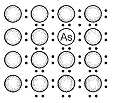
(b) 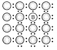
(c) 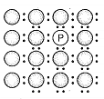
(d) 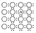
NEETprep Answer
48. Which of the following statements are correct?
(a) Ferrimagnetic substances lose ferrimagnetism on heating and become paramagnetic
(b) Ferrimagnetic substances do not lose ferrimagnetism on heating and remain ferrimagnetic
(c) Antiferromagnetic substances have domain structures similar to ferromagnetic substances and their magnetic moments are not cancelled by each other
(d) In ferromagnetic substances, all the domains get oriented in the direction of magnetic field and remain as such even after removing magnetic field
NEETprep Answer
49. Whichof the following features are not shown by quartz glass?
(a) This is a crystalline solid
(b) Refractive index is same in ail the directions
(c) This has definite heat of fusion
(d) This is also called super cooled liquid
NEETprep Answer
50. Which of the following cannot be regarded as molecular solid?
(a) SiC (silicon carbide)
(b) AlN
(c) Diamond
(d) I2
NEETprep Answer
51. In which of the following arrangements octahedral voids are formed?
(a) hcp
(b) bcc
(c) simple cubic
(d) fcc
NEETprep Answer
52. Frenkel defect is also known as.......... .
(a) stoichiometric defect
(b) disiocation defect
(c) impurity defect
(d) non-stoichiometric defect
NEETprep Answer
53. Which of the following defects decrease the density?
(a) Interstitial defect
(b) Vacancy defect
(c) Frenkel defect
(d) Schottky defect
NEETprep Answer
Short Answer Type Questions
54. Why are liquids and gases categorised as fluids?
NEETprep Answer
55. Why are solids incompressible?
NEETprep Answer
56. Inspite of long range order in the arrangement of particles why are the crystals usually not perfect?
NEETprep Answer
57. Why doestable salt, NaCl sometimes appear yellow in colour?
NEETprep Answer
58. Why is FeO(s) not formed in stoichiometric composition?
NEETprep Answer
59. Why does white ZnO (s) becomes yellow upon heating?
NEETprep Answer
60. Why does the electrical conductivity of semiconductors increase with rise in temperature?
NEETprep Answer
61. Explain why does conductivity of germanium crystals increase on doping with galium?
NEETprep Answer
62. In a compound, nitrogen atoms (N) make cubic close packed lattic and metal atoms (M) occupy one-third of the tetrahedral voids present. Determine the formula of the compound formed by M and N?
NEETprep Answer
63. Under which situations can an amorphous substance change to crystalline form ?
NEETprep Answer
Matching The Columns
64. Match the defects given in Column I with the statements in given Column II.
|
Column I |
Column II |
|
A. B. C. D. |
Simple vacancy defect Simple interstitial defect Frenkel defect Schottky defect |
1. Shown by non-ionic solids and increases density ofthe solid 2. Shown byionic solids and decreases density of the solid 3. Shown by non-ionic solids and density of the solid decreases 4. Shown byionic solids and density of the solid remains the same |
65. Match the type of unit cell given in Column I with the features given in Column II.
Column I |
Column II |
|
A. Primitive cubic unit cell B. Body centred cubic unit cell C. Face centred cubic unit cell D. End centred orthorhombic |
1. Each of the three perpendicular edges compulsorily have the different edge length i.e., abc 2. Number of atoms per unit cell is one. 3. Each of the three perpendicular edges compulsorily have the same edge length i.e., a=b=c 4. In addition to the contribution from the corner unit cell atoms the number of atoms present in a unit cell is one 5. In addition to the contribution from the corner atoms the number of atoms present in a unit cell is three |
66. Match the types of defect given in Column I with the statement given in Column II.
Column I |
Column II |
|
A. Impurity defect B. Metal excess defect C. Metal deficiency defect |
1. NaCl with anionic sites called F-centres 2. FeO with Fe3+ 3. NaCl with Sr2+ and some cationic sites vacant |
67. Match the items given in Column I with the items given in Column II.
Column I |
Column II |
|
A. Mg in solid state B. MgCl2 in molten state C. Silicon with phosphorus D. Germanium with boron |
1. p-type semiconductor 2. n-type semiconductor 3. Electrolytic conductors 4. Electronic conductors |
68. Match the type of packing given in Column I with the items given in Column II.
Column I |
Column II |
|
A. Square close packing in two dimensions B. Hexagonal close packing in two dimensions C. Hexagonal close packing in three dimensions D. Cubic close packing in three dimensions |
1. Triangular voids 2. Pattern of spheres is repeated in every fourth layer 3. Coordination number =4 4. Pattern of sphere is repeated in alternate layers |
Assertion and Reason
In the following questions a statement of Assertion (A) followed by a statement of Reason (R) is given. Choose the correct answer out of the following choices.
(a) Assertion and Reason both are correct statements and Reason is correct explanation for Assertion.
(b) Assertion and Reason both are correct statements but Reason is not correct explanation for Assertion.
(c) Assertion is correct statement but Reason is wrong statement.
(d) Assertion is wrong statement but Reason is correct statement.
69. Assertion (A) The total number of atoms present in a simple cubic unit cell is one.
Reason (R) Simple cubic unit cell has atoms at its corners, each of which is shared between eight adjacent unit cells.
70. Assertion (A) Graphite is a good conductor of electricity however diamond belongs to the category of insulators.
Reason (R) Graphite is soft in nature on the other hand diamond is very hard and brittle.
71. Assertion (A) Total number of octahedral voids present in unit cell of cubic close packing including the one that is present at the body centre, is four.
Reason (R) Besides the body centre there is one octahedral void present at the centre of each of the six faces of the unit cell and each of which is shared between two adjacent unit cells.
72. Assertion (A) The packing efficiency is maximum for the fcc structure.
Reason (R) The coordination numberis 12 in fcc structures.
73. Assertion(A) Semiconductors are solids with conductivities in the range from 10-6 — 104 ohm-1 m-1 .
Reason (R) Intermediate conductivity in semiconductor is due to partially filled valence band.
Long Answer Type Questions
74. With the help of a labelled diagram show that there are four octahedral voids per unit cell in a cubic close packed structure.
75. Show that in a cubic close packed structure, eight tetrahedral voids are present per unit cell.
76. How does the doping increase the conductivity of semiconductors?
77. A sample of ferrous oxide has actual formula Fe0.93O1.00 . In this sample, what fraction of metal ions are Fe2+ ions? What type of non-stoichiometric defect is present in this sample?
© 2026 GoodEd Technologies Pvt. Ltd.


