 Q. No.
Let and be the number of holes and conduction electrons respectively in a semiconductor. Then
(1) > in an intrinsic semiconductor
(2) = in an extrinsic semiconductor
(3) = in an intrinsic semiconductor
(4) < in an intrinsic semiconductor


The energy gap of silicon is 1.14 eV. The maximum wavelength at which silicon will begin absorbing energy is
(1) 10888 Å
(2) 1088.8 Å
(3) 108.88 Å
(4) 10.888 Å


The diagrams below show energy band structures for three silicon semiconductor samples labelled \(X,Y,\) and \(Z.\)

Based on these energy band diagrams, which statement correctly identifies the doping type for each sample?
| 1. | Sample \(X\) is undoped, while samples \(Y\) and \(Z\) have been doped with third-group and fifth-group impurities, respectively. |
| 2. | Sample \(X\) is undoped, while both samples \(Y\) and \(Z\) have been doped with fifth-group impurities. |
| 3. | Sample \(X\) has been doped with equal amounts of third- and fifth-group impurities, while samples \(Y\) and \(Z\) are undoped. |
| 4. | Sample \(X\) is undoped, while samples \(Y\) and \(Z\) have been doped with fifth-group and third-group impurities, respectively. |
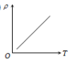
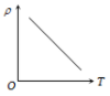
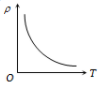
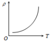
The temperature (T) dependence of resistivity () of a semiconductor is represented by
1. 
2. 
3. 
4. 
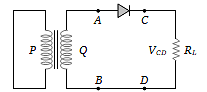
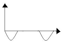
In the half-wave rectifier circuit shown. Which one of the following wave forms is true for , the output across C and D?
| 1. | 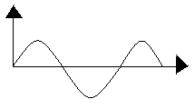 |
2. | 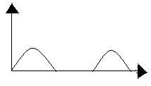 |
| 3. | 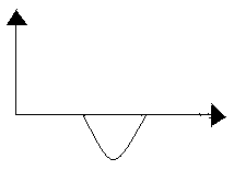 |
4. |  |


Zener diode is used for:-
1. Rectification
2. Stabilisation
3. Amplification
4. Producing oscillations in an oscillator
The logic behind the ‘NOR’ gate is that it gives
(1) High output when both the inputs are low
(2) Low output when both the inputs are low
(3) High output when both the inputs are high
(4) None of these


The combination of ‘NAND’ gates shown here under (figure) are equivalent to

1. An OR gate and an AND gate respectively
2. An AND gate and a NOT gate respectively
3. An AND gate and an OR gate respectively
4. An OR gate and a NOT gate respectively.
© 2026 GoodEd Technologies Pvt. Ltd.