
 Q. No.
The given electrical network is equivalent to:

1.
\(\text{OR}\) gate
2.
\(\text{NOR}\) gate
3.
\(\text{NOT}\) gate
4.
\(\text{AND}\) gate


What is the output \(Y\) in the following circuit, when all the three inputs \(A\), \(B\), and \(C\) are first \(0\) and then \(1\)?
1. \(0,1\)
2. \(0,0\)
3. \(1,0\)
4. \(1,1\)


To get output \(Y=1\) for the following circuit, the correct choice for the input is:

| 1. | \(A=1,~ B= 0, ~C=0\) |
| 2. | \(A=1,~ B= 1, ~C=0\) |
| 3. | \(A=1,~ B= 0, ~C=1\) |
| 4. | \(A=0,~ B= 1, ~C=0\) |
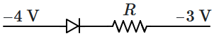
Consider the junction diode as an ideal. The value of current flowing through \(AB\) is:
1. \(10^{-2}~\text{A}\)
2. \(10^{-1}~\text{A}\)
3. \(10^{-3}~\text{A}\)
4. \(0~\text{A}\)

The input signal given to a CE amplifier having a voltage gain of 150 is . The corresponding output signal will be:
1.
2.
3.
4.


If in a \(\mathrm{p\text{-}n}\) junction, a square input signal of \(10~\text{V}\) is applied as shown,
then the output across \(R_L\) will be:

| 1. |  |
2. |  |
| 3. |  |
4. |  |
Which logic gate is represented by the following combination of logic gates?

2. \(\mathrm{NAND}\)
3. \(\mathrm{AND}\)
4. \(\mathrm{NOR}\)
The given graph represents the \(\mathrm{V\text{-} I}\) characteristic for a semiconductor device.
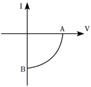
Which of the following statement is correct?
| 1. | It is a \(\mathrm{V\text{-} I}\) characteristic for the solar cell where point \(\mathrm{A}\) represents open-circuit voltage and point \(\mathrm{B}\) short circuit current. |
| 2. | It is for a solar cell and points \(\mathrm{A}\) and \(\mathrm{B}\) represent open-circuit voltage and current, respectively. |
| 3. | It is for a photodiode and points \(\mathrm{A}\) and \(\mathrm{B}\) represent open-circuit voltage and current respectively. |
| 4. | It is for a LED and points \(\mathrm{A}\) and \(\mathrm{B}\) represent open circuit voltage and short circuit current, respectively. |


| 1. | Electrons are minority carriers and pentavalent atoms are dopants. |
| 2. | Holes are minority carriers and pentavalent atoms are dopants. |
| 3. | Holes are the majority carriers and trivalent atoms are dopants. |
| 4. | Electrons are the majority carriers and trivalent atoms are dopants. |
© 2026 GoodEd Technologies Pvt. Ltd.