
 Q. No.
In the combination of the following gates, the output \(Y\) can be written in terms of inputs \(A\) and \(B\) as:

1. \(\overline {A\cdot B}\)
2. \(A\cdot \overline{B}+ B\cdot \overline{A}\)
3. \(\overline {A\cdot B}+ A\cdot B\)
4. \(\overline {A+ B}\)
1. \(\overline {A\cdot B}\)
2. \(A\cdot \overline{B}+ B\cdot \overline{A}\)
3. \(\overline {A\cdot B}+ A\cdot B\)
4. \(\overline {A+ B}\)


In the circuit shown in the figure, the input voltage Vi is 20 V, VBE = 0, and VCE = 0. The values of IB, IC and are given by:

1.
2.
3.
4.
In a \(\mathrm{p\text{-}n}\) junction diode, the change in temperature due to heating:
| 1. | affects only reverse resistance. |
| 2. | affects only forward bias. |
| 3. | does not affect the resistance of the \(\mathrm{p\text{-}n}\) junction. |
| 4. | affects the overall \(\mathrm{V\text{-}I}\) characteristics of a \(\mathrm{p\text{-}n}\) junction. |


The given electrical network is equivalent to:

| 1. | \(\text{OR}\) gate | 2. | \(\text{NOR}\) gate |
| 3. | \(\text{NOT}\) gate | 4. | \(\text{AND}\) gate |


What is the output \(Y\) in the following circuit, when all the three inputs \(A\), \(B\), and \(C\) are first \(0\) and then \(1\)?
1. \(0,1\)
2. \(0,0\)
3. \(1,0\)
4. \(1,1\)


To get output \(Y=1\) for the following circuit, the correct choice for the input is:

| 1. | \(A=1,~ B= 0, ~C=0\) |
| 2. | \(A=1,~ B= 1, ~C=0\) |
| 3. | \(A=1,~ B= 0, ~C=1\) |
| 4. | \(A=0,~ B= 1, ~C=0\) |
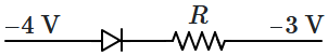
Consider the junction diode as an ideal. The value of current flowing through \(AB\) is:
1. \(10^{-2}~\text{A}\)
2. \(10^{-1}~\text{A}\)
3. \(10^{-3}~\text{A}\)
4. \(0~\text{A}\)

The input signal given to a CE amplifier having a voltage gain of 150 is . The corresponding output signal will be:
1.
2.
3.
4.


If in a \(\mathrm{p\text{-}n}\) junction, a square input signal of \(10~\text{V}\) is applied as shown,
then the output across \(R_L\) will be:

| 1. |  |
2. |  |
| 3. |  |
4. |  |
© 2026 GoodEd Technologies Pvt. Ltd.