In a CE transistor amplifier, the audio signal voltage across the collector resistance of 2 If the base resistance is 1 and the current amplification of the transistor is 100, the input signal voltage is
1. 0.1 V
2. 1.0 V
3. 1mV
4. 10mV
2. 1.0 V
3. 1mV
4. 10mV
C and Si both have same lattice structure,having 4 bonding electrons in each.However, C is insulator whereas Si is intrinsic semiconductor. This is because
1. in case of C, the valence band is not completely filled at absolute zero temperature
2. in case of C,the condition band is partly filled even at absolute zero temperature
3. the four bonding electrons in the case of C lie in the second orbit,Whereas in the case of Si they lie in the third
4 .the four bonding electrons in the case of C lie in the third orbit, whereas for Si they lie in the fourth orbit
The figure shows a logic circuit with two inputs A and B and the output C. The voltage wave forms across A, B and C are as given. The logic circuit gate is
1. OR gate
2. NOR gate
3. AND gate
4. NAND gate
The input resistance of a silicon transistor is
100 . Base current is changed by 40
which results in a change in collector current
by 2 mA. This transistor is used as a common-
emitter amplifier with a load resistance of 4 k.
The voltage gain of the amplifier is
1. 2000
2. 3000
3. 4000
4. 1000
To get an output Y=1 in given circuit, which
of the following input will be correct ?
A B C
1. 1 0 0
2. 1 0 1
3. 1 1 0
4. 0 1 0
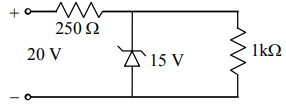
A Zener diode, having breakdown voltage equal to \(15\) V, is used in a voltage regulator circuit, as shown in the figure. The current through the diode is:

1. \(10\) mA
2. \(15\) mA
3. \(20\) mA
4. \(5\) mA
The device that can act as a complete electronic circuit is
1. Junction diode
2. Integrated circuit
3. Junction transistor
4. Zener diode
A transistor is operated in common-emitter configuration at such that a change in the base current from 100 to 200 produces a change in the collector current from 5 mA to 10 mA. The current gain is
1. 75
2. 100
3. 150
4. 50
A p-n photodiode is made of a material with a band gap of 2.0 eV. The minimum frequency of the radiation that can be absorbed by the material is nearly
1.
2.
3.
4.
The circuit is equivalent to
1. AND gate 2. NAND gate
3. NOR gate 4. OR gate


