
 Q. No.
Which material is preferred for solar cells?
1. \(\text{Si}\)
2. \(\text{GaAs}\)
3. \(\text{CdS}\)
4. both \(\text{Si}\) and \(\text{GaAs}\)
1. \(\text{Si}\)
2. \(\text{GaAs}\)
3. \(\text{CdS}\)
4. both \(\text{Si}\) and \(\text{GaAs}\)


Graph shows barrier potential for a p-n junction diode under different biasing conditions where Vo is the built-in potential of the diode. Then graph 2 represents:

1. Forward biasing with low voltage battery
2. Forward biasing with high voltage battery
3. Reverse biasing
4. Unbiased condition

The output characteristics of a transistor are shown in the figure. When is \(10\) V and = \(4.0\) mA, the value of is:

1. \(200\)
2. \(250\)
3. \(150\)
4. \(100\)


The output waveform \((Y) \)of the AND gate for the following inputs \(A\) and \(B \) given in the figure, is:

| 1. |  |
| 2. |  |
| 3. |  |
| 4. | None of these |
The output waveform \((Y)\) of the NAND gate for the following inputs \(A\) and \(B\) given in the figure is:

| 1. | |
| 2. | |
| 3. | |
| 4. | none of these |
For a Silicon CE transistor amplifier, the audio signal voltage across the collector resistance of 2.0 k is 2.0 V. Suppose the current amplification factor of the transistor is 100, what should be the value of in series with the supply of 2.0 V if the dc base current has to be 10 times the signal current?
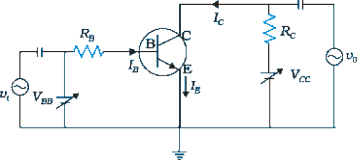


For a Silicon CE transistor amplifier, the audio signal voltage across the collector resistance of 2.0 k is 2.0 V. Suppose the current amplification factor of the transistor is 100 if the dc base current has to be 10 times the signal current. The dc current across through the collector resistance will be:
1. 0.1 mA
2. 10 mA
3. 1.0 mA
4. 0.01 mA
In figure, the supply can be varied from 0 V to 5.0 V. The Si transistor has = 250 and = 100 k, = 1 K, = 5.0 V. Assume that when the transistor is saturated, = 0 V and = 0.8V. The minimum base current, for which the transistor will reach saturation is:
In figure, the supply can be varied from 0 V to 5.0 V. The Si transistor has = 250 and = 100 k, = 1 K, = 5.0 V. Assume that when the transistor is saturated, = 0 V and = 0.8V. The input voltage for which the transistor will reach saturation is:
1. 0.8 V
2. 5.0 V
3. 2.8 V
4. 1.4 V


The electron concentration in an \(\mathrm{n\text-}\)type semiconductor is the same as the hole concentration in a \(\mathrm{p\text{-}}\)type semiconductor. An external field (electric) is applied across each of them. Compare the currents in them.
| 1. | current in \(\mathrm{n\text-}\)type \(>\) current in \(\mathrm{p\text{-}}\)type. |
| 2. | no current will flow in \(\mathrm{p\text{-}}\)type, current will only flow in \(\mathrm{n\text-}\)type. |
| 3. | current in \(\mathrm{n\text-}\)type \(=\) current in \(\mathrm{p\text{-}}\)type. |
| 4. | current in \(\mathrm{p\text{-}}\)type \(>\) current in \(\mathrm{n\text-}\)type. |
© 2026 GoodEd Technologies Pvt. Ltd.