 Q. No.
The contribution in the total current flowing through a semiconductor due to electrons and holes are and respectively. If the drift velocity of electrons is times that of holes at this temperature, then the ratio of concentration of electrons and holes is
1. 6 : 5
2. 5 : 6
3. 3 : 2
4. 2 : 3
इलेक्ट्रॉनों और कोटरों के कारण एक अर्धचालक के माध्यम से बहने वाली कुल धारा में क्रमशः और का योगदान है। यदि इलेक्ट्रॉनों का अपवाह वेग इस तापमान पर कोटरों के अपवाह वेग का गुना है, तो इलेक्ट्रॉनों और कोटरों की सांद्रता का अनुपात है:
(1) 6: 5
(2) 5: 6
(3) 3: 2
(4) 2: 3
1. 6 : 5


Figure gives a system of logic gates. From the study of truth table it can be found that to produce a high output (1) at R, we must have

(a) X = 0, Y = 1
(b) X = 1, Y = 1
(c) X = 1, Y = 0
(d) X = 0, Y = 0
आरेख लॉजिक गेट की प्रणाली दर्शाता है। सत्यता सारणी के अध्ययन से यह पाया जा सकता है कि R पर उच्च निर्गत (1) प्राप्त करने के लिए, हमें प्राप्त होना चाहिए:
(a) X = 0, Y = 1
(b) X = 1, Y = 1
(c) X = 1, Y = 0
(d) X = 0, Y = 0
A transistor is operated in common emitter configuration at When base current is changed from 10mA to 30mA, it produces a change in emitter current from 2A to 4A, the current amplification factor is
1. 100
2. 99
3. 10
4. 9
एक ट्रांजिस्टर उभयनिष्ठ उत्सर्जक विन्यास में पर संचालित किया जाता है। जब आधार धारा को 10mA से 30mA में परिवर्तित किया जाता है, तब यह उत्सर्जक धारा में 2A से 4A का परिवर्तन उत्पन्न करता है। धारा प्रवर्धन कारक है
1. 100
2. 99
3. 10
4. 9


An LED is constructed from a p-n junction diode using GaAsP. The energy gap is 1.9 eV. The wavelength of the light emitted will be equal to:
1. 10.4
2. 654 nm
3. 654 m
4. 654
GaAsP का उपयोग करके एक p-n संधि डायोड से एक LED का निर्माण किया जाता है। ऊर्जा का अंतर 1.9 eV है। उत्सर्जित प्रकाश की तरंग दैर्ध्य इसके बराबर होगी:
1. 10.4
2. 654 एनएम
3. 654 m
4. 654


The input signal is given to a CE amplifier having a voltage gain of 150 is . The corresponding output signal will be:
1.
2.
3.
4.
CE प्रवर्धक को दिए गए निवेशी सिग्नल में 150 का वोल्टेज लाभ है। संगत निर्गत सिग्नल होगा:
1.
2.
3.
4.


In the given figure, potential difference between A and B is

(1) 0
(2) 5 volt
(3) 10 volt
(4) 15 volt
दिए गए आरेख में, A और B के मध्य विभवांतर कितना है?
(1) 0
(2) 5 volt
(3) 10 volt
(4) 15 volt
Least doped region in a transistor
(a) Either emitter or collector
(b) Base
(c) Emitter
(d) Collector
ट्रांजिस्टर में न्यूनतम अपमिश्रित क्षेत्र कौन-सा होता है?
(a) या तो उत्सर्जक या संग्राहक
(b) आधार
(c) उत्सर्जक
(d) संग्राहक
In a forward biased PN-junction diode, the potential barrier in the depletion region is of the form
1. 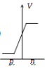
2. 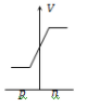
3. 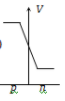
4. 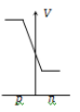
अग्र अभिनत PN संधि डायोड में, अवक्षय पर्त में विभव प्राचीर का रूप है:


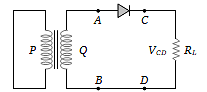
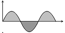
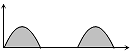
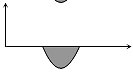
In the half-wave rectifier circuit shown. Which one of the following wave forms is true for , the output across C and D?
1. 
2. 
3. 
4. 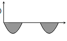
दिखाए गए अर्द्ध तरंग दिष्टकारी में, निम्नलिखित तरंग रूपों में से कौन सा C और D पर निर्गत के लिए सही है?

© 2026 GoodEd Technologies Pvt. Ltd.