 Q. No.
In the following circuit, find and .

(a) 0, 0
(b) 5 mA, 5 mA
(c) 5 mA, 0
(d) 0, 5 mA
निम्नलिखित परिपथ में, और ज्ञात कीजिए:
(a) 0, 0
(b) 5 mA, 5 mA
(c) 5 mA, 0
(d) 0.5 mA
(b) 5 mA, 5 mA
(c) 5 mA, 0
(d) 0, 5 mA
(b) 5 mA, 5 mA
(c) 5 mA, 0
(d) 0.5 mA


The cut-in voltage for silicon diode is approximately
(a) 0.2 V (b) 0.6 V
(c) 1.1 V (d) 1.4 V
सिलिकॉन डायोड के लिए भंजक वोल्टता लगभग है:
(a) 0.2 V (b) 0.6 V
(c) 1.1 V (d) 1.4 V
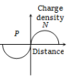
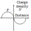
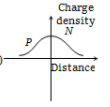
The curve between charge density and distance near P-N junction will be
1. 
2. 
3. 
4. 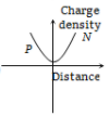
P-N संधि के निकट आवेश घनत्व और दूरी के बीच का वक्र कौन-सा होगा?
1.
2.
3.
4.


The valency of the impurity atom that is to be added to germanium crystal so as to make it an N-type semiconductor, is
(1) 6
(2) 5
(3) 4
(4) 3
अपमिश्रित परमाणु की संयोजकता ज्ञात कीजिए, जिसे जर्मेनियम क्रिस्टल में मिलाने पर इसे N-प्रकार अर्धचालक बनाया जा सकता है।
(1) 6
(2) 5
(3) 4
(4) 3
The valence of an impurity added to germanium crystal in order to convert it into a P-type semiconductor is
(1) 6
(2) 5
(3) 4
(4) 3
जर्मेनियम क्रिस्टल को p-प्रकार अर्धचालक में परिवर्तित करने के लिए कितनी संयोजकता के अपद्रव्य को मिलाया जाता है?
(1) 6
(2) 5
(3) 4
(4) 3
The symbol given in figure represents

(a) NPN transistor
(b) PNP transistor
(c) Forward biased PN junction diode
(d) Reverse biased NP junction diode
आरेख में दर्शाया गया प्रतीक किसको दर्शाता है?
(a) NPN ट्रांजिस्टर
(b) PNP ट्रांजिस्टर
(c) अग्र अभिनत PN संधि डायोड
(d) उत्क्रम अभिनत NP संधि डायोड


Function of rectifier is
| 1. | To convert ac into dc |
| 2. | To convert dc into ac |
| 3. | Both (a) and (b) |
| 4. | None of these |
दिष्टकारी का कार्य है -
| 1. | AC को DC में परिवर्तित करना |
| 2. | DC को AC में परिवर्तित करना |
| 3. | (a) और (b) दोनों |
| 4. | इनमें से कोई नहीं |
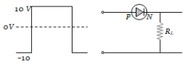
If the following input signal is sent through a PN-junction diode, then the output signal across will be
1. 
2. 
3. 
4. 
यदि PN-संधि डायोड के माध्यम से निम्नलिखित निवेश सिग्नल भेजा जाता है, तब के मध्य निर्गत सिग्नल क्या होगा?

The given figure shows the wave forms for two inputs A and B and that for the output Y of a logic circuit. The logic circuit is

(a) An AND gate (b) An OR gate
(c) A NAND gate (d) An NOT gate
दिया गया आरेख दो निवेशी A और B के लिए तरंग रूपों और लॉजिक परिपथ के निर्गत Y को दर्शाता है। लॉजिक परिपथ है:
(a) AND गेट (b) OR गेट
(c) NAND गेट (d) NOT गेट


Two ideal diodes are connected to a battery as shown in the circuit. The current supplied by the battery is

(a)0.75A (b)zero
(c)0.25A (d)0.5A
दो आदर्श डायोडों को बैटरी के साथ दर्शाए गए परिपथ अनुसार जोड़ा गया है। बैटरी द्वारा आपूर्ति की जाने वाली धारा की गणना कीजिए:
(a) 0.75A (b) शून्य
(c) 0.25A (d) 0.5A
© 2026 GoodEd Technologies Pvt. Ltd.