
 Q. No.
Logic gates X and Y have the truth tables shown below:
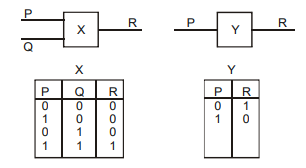
When the output of X is connected to the input of Y, the resulting combination is equivalent to a single:
1. NOT gate
2. OR gate
3. NAND gate
4. AND gate


The depletion layer in the P–N junction region is caused by:
| 1. | the drift of holes |
| 2. | diffusion of charge carriers |
| 3. | migration of impurity ions |
| 4. | drift of electrons |


In the given circuit, PN-junction diodes are ideal. For the following potential of A and B, the correct increasing order of resistance between A and B will be:

i. –10V, –5V
ii. –5V, –10V
iii. –4V, –12V
1. (i) < (ii) < (iii)
2. (iii) < (ii) < (i)
3. (ii) = (iii) < (i)
4. (i) = (iii) < (ii)
The combination of gates shown below is equivalent to:
1. AND gate

2. XOR gate
3. NOR gate
4. NAND gate
The given circuit has two ideal diodes connected as shown in the figure below. The current flowing through the resistance R1 will be:

| 1. | 2.5 A | 2. | 10.0 A |
| 3. | 1.43 A | 4. | 3.13 A |
In the energy band diagram of a material shown below, the open circles and filled circles denote holes and electrons respectively. The material is a/an:

| 1. | p-type semiconductor |
| 2. | insulator |
| 3. | metal |
| 4. | n-type semiconductor |
The LED:
1. is reverse-biased.
2. is forward-biased.
3. can be made of GaAs.
4. both (2) & (3) are correct.
In the circuit shown, are respectively:
(If diodes are ideal)

1. 0, 0
2. 5 mA, 5 mA
3. 5 mA, 0
4. 0, 5 mA
The output of the OR gate is 1:
1. only if both inputs are zero.
2. if either or both inputs are 1.
3. only if both inputs are 1.
4. if any of the inputs is zero.
© 2024 GoodEd Technologies Pvt. Ltd.