 Q. No.
Transfer characteristic [output voltage vs input voltage ] for a base biased transistor in CE configuration is as shown in the figure. For using transistor as a switch, it is used:

1. in region III
2. both in region (I) and (III)
3. in region II
4. in region I


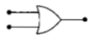
The figure shows a logic circuit with two inputs A and B and the output C.The voltage wave forms across A, B and C are as given.The logic circuit gate is

1. OR gate 2. NOR gate
3. AND gate 4. NAND gate
The input resistance of a silicon transistor is
100 . Base current is changed by 40
which results in a change in collector current
by 2 mA. This transistor is used as a common-
emitter amplifier with a load resistance of 4 k.
The voltage gain of the amplifier is
1. 2000
2. 3000
3. 4000
4. 1000


Symbolic representation of four logic gates
are shown as
(i)
(ii)

(iii)

(iv)
Pick out which ones are for AND, NAND and
NOT gates, respectively.
(a) (iii), (ii)and (i)
(b) (iii), (ii) and (iv)
(c) (ii), (iv) and (iii)
(d) (ii), (iii) and (iv)
If a small amount of antimony is added to germanium crystal
(1) the antimony becomes an acceptor atom
(2) there will be more free electrons than holes in the semiconductor
(3) its resistance is increased
(4) it becomes a p-type semiconductor
In forward biasing of the p-n junction
| 1. | the positive terminal of the battery is connected to n-side and the depletion region becomes thin |
| 2. | the positive terminal of the battery is connected to n-side and the depletion region becomes thick |
| 3. | the positive terminal of the battery is connected to p-side and the depletion region becomes thin |
| 4. | the positive terminal of the battery is connected to p-side and the depletion region becomes thick |
The decreasing order of the wavelength of infrared, microwave, ultraviolet and gamma rays is
(1) gamma rays, ultraviolet, infrared, microwaves
(2) microwaves, gamma rays, infrared, ultraviolet
(3) infrared, microwave, ultraviolet, gamma rays
(4) microwave, infrared, ultraviolet, gamma rays
In the following figure, the diodes which are forward biased, are


1. III and IV only
2. I and III only
3. II only
4. II and IV only
Pure Si at 500 K has equal number of electron and hole concentration of Doping by indium increases to The doped semiconductor is of:
| 1. | n-type with electron concentration \(n_{e}=5\times10^{22}~m^{-3}\) |
| 2. | p-type with electron concentration \(n_{e}=2.5\times10^{23}~m^{-3}\) |
| 3. | n-type with electron concentration \(n_{e}=2.5\times10^{10}~m^{-3}\) |
| 4. | p-type with electron concentration \(n_{e}=5\times10^{9}~m^{-3}\) |
A Zener diode, having breakdown voltage equal to 15 V, is used in a voltage regulator circuit, as shown in the figure. The current through the diode is:
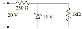
1. 10 mA
2. 15 mA
3. 20 mA
4. 5 mA
© 2024 GoodEd Technologies Pvt. Ltd.