 Q. No.
A transistor is used in common emitter mode in an amplifier circuit. When a signal of 10 mV is added to the base-emitter voltage, the base current changes by 15 A and the collector current changes by 1.5 mA. The current gain \(\beta\) will be:
1. 50
2. 48
3. 100
4. 200


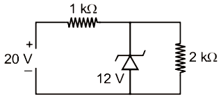
| 1. | \(5~\text A\) | 2. | \(0.2~\text A\) |
| 3. | \(0.6~\text A\) | 4. | zero |


In a common emitter transistor amplifier, the audio signal vlotage across the collector is 3V. The resistance of collector is 3k. If current gain is 100 and the base resistance is 2k, the voltage and power gain of the amplifier is
(1) 200 and 1000
(2) 15 and 200
(3) 150 and 15000
(4) 20 and 2000
What is the output Y in the following circuit, when all the three inputs A,B,C are first 0 and then 1 ?

1. 0,1 2. 0,0
3. 1,0 4. 1,1


Which logic gate is represented by the following combination of logic gates?

1. OR
2. NAND
3. AND
4. NOR
In the given figure, a diode D is connected to an external resistance R = 100 Ω and an e.m.f of 3.5 V. If the barrier potential developed across the diode is 0.5 V, the current in the circuit will be
1. 30mA
2. 40mA
3. 20mA
4. 35mA

The barrier potential of a p-n junction depends on
(i)type of semiconductor material
(ii)amount of doping
(iii)temperature
Which one of the following is correct
1. (i) and (ii)only
2. (ii) only
3. (ii) and (iii)only
4. (i),(ii) and (iii)


C and Si both have same lattice structure,having 4 bonding electrons in each.However, C is insulator whereas Si is intrinsic semiconductor. This is because
1. in case of C, the valence band is not completely filled at absolute zero temperature
2. in case of C,the condition band is partly filled even at absolute zero temperature
3. the four bonding electrons in the case of C lie in the second orbit,Whereas in the case of Si they lie in the third
4 .the four bonding electrons in the case of C lie in the third orbit, whereas for Si they lie in the fourth orbit
© 2025 GoodEd Technologies Pvt. Ltd.