
 Q. No.
In the following circuit, the output \(Y\) for all possible inputs \(A\) and \(B\) is expressed by the truth table:

1.
A
B
Y
2.
A
B
Y
0
0
0
0
0
1
0
1
0
0
1
1
1
0
0
1
0
1
1
1
1
1
1
0
3.
0
0
1
4.
0
0
0
0
1
0
0
1
1
1
0
0
1
0
1
1
1
1
1
1
1


In the energy band diagram of a material shown below, the open circles and filled circles denote holes and electrons respectively. The material is a/an:
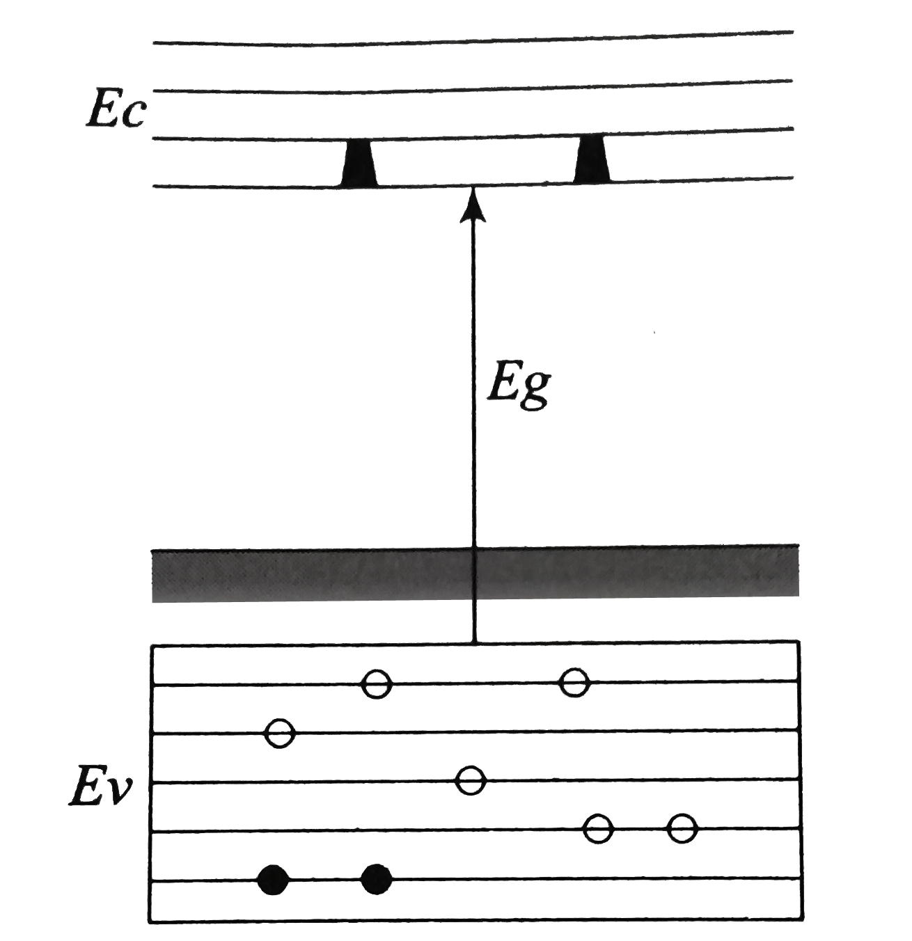
1. p-type semiconductor
2. insulator
3. metal
4. n-type semiconductor


The following figure shows a logic gate circuit with two inputs A and B and the output C. The voltage waveforms of A, B, and C are as shown below:
The logic circuit gate is:

1. AND gate
2. NAND gate
3. NOR gate
4. OR gate
For a \(\mathrm{p}\text{-}\)type semiconductor, which of the following statements is true?
| 1. | Electrons are the majority carriers and pentavalent atoms are the dopants. |
| 2. | Electrons are the majority carriers and trivalent atoms are the dopants. |
| 3. | Holes are the majority carriers and trivalent atoms are the dopants. |
| 4. | Holes are the majority carriers and pentavalent atoms are the dopants. |
The correct Boolean operation represented by the circuit diagram given above is:
1. \(\mathrm{NOR}\)
2. \(\mathrm{AND}\)
3. \(\mathrm{OR}\)
4. \(\mathrm{NAND}\)


A p-n photodiode is made of a material with a bandgap of 2.0 eV. The minimum frequency of the radiation that can be absorbed by the material is nearly:
1.
2.
3.
4.
The symbolic representation of four logic gates is as shown:
| (i) |  |
(ii) |  |
| (ii) |  |
(iv) |  |
The logic symbols for OR, NOT, and NAND gates are respectively:
1. (iii), (iv), (ii)
2. (iv), (i), (iii)
3. (iv), (ii), (i)
4. (i), (iii), (iv)


1. \(6000~\mathring{A}\)
2. \(4000~\text{nm}\)
3. \(6000~\text{nm}\)
4. \(4000~\mathring{A}\)
© 2025 GoodEd Technologies Pvt. Ltd.