
 Q. No.
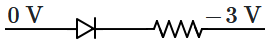
The circuit diagram shown here corresponds to the logic gate:

1. \(\text{NOR}\)
2. \(\text{AND}\)
3. \(\text{OR}\)
4. \(\text{NAND}\)
1. \(\text{NOR}\)
2. \(\text{AND}\)
3. \(\text{OR}\)
4. \(\text{NAND}\)


An LED is constructed from a \(\mathrm{p\text{-}n}\) junction diode using \(\mathrm{GaAsP}.\) The energy gap is \(1.9~\text{eV}.\) The wavelength of the light emitted will be equal to:
1. \(10.4 \times 10^{-26}~ \text{m}\)
2. \(654~ \text{nm}\)
3. \(654~ \text{m}\)
4. \(654\times 10^{-11}~\text{m}\)
The correct Boolean operation represented by the circuit diagram given above is:
1. \(\mathrm{NOR}\)
2. \(\mathrm{AND}\)
3. \(\mathrm{OR}\)
4. \(\mathrm{NAND}\)


For a \(\mathrm{p}\text{-}\)type semiconductor, which of the following statements is true?
| 1. | Electrons are the majority carriers and pentavalent atoms are the dopants. |
| 2. | Electrons are the majority carriers and trivalent atoms are the dopants. |
| 3. | Holes are the majority carriers and trivalent atoms are the dopants. |
| 4. | Holes are the majority carriers and pentavalent atoms are the dopants. |
For the logic circuit shown, the truth table is:

| 1. |
|
|||||||||||||||
| 2. |
|
|||||||||||||||
| 3. |
|
|||||||||||||||
| 4. |
|
The increase in the width of the depletion region in a \(\mathrm{p\text{-}n}\) junction diode is due to:
1. reverse bias only
2. both forward bias and reverse bias
3. increase in forwarding current
4. forward bias only


The solids which have the negative temperature coefficient of resistance are:
| 1. | insulators only |
| 2. | semiconductors only |
| 3. | insulators and semiconductors |
| 4. | metals |


Which of the following gate is called the universal gate?
1. \(\mathrm{OR}\) gate
2. \(\mathrm{AND}\) gate
3. \(\mathrm{NAND}\) gate
4. \(\mathrm{NOT}\) gate
An intrinsic semiconductor is converted into an \(\mathrm{n\text{-}}\)type extrinsic semiconductor by doping it with:
1. phosphorous
2. aluminium
3. silver
4. germanium
© 2025 GoodEd Technologies Pvt. Ltd.