Select Chapter Topics:

 Q. No.
What is the reading of the ideal ammeters \(A_1\) and \(A_2\) connected in the given circuit diagram, if \(\mathrm{p\text-n}\) junction diodes are ideal?

1.
\(2~\text A\) and zero
2.
\(3~\text A\) and \(2~\text A\)
3.
\(2~\text A\) and \(3~\text A\)
4.
Zero and \(2~\text A\)


Subtopic: PN junction |
84%
From NCERT
To view explanation, please take trial in the course.
NEET 2026 - Target Batch - Vital
Hints
To view explanation, please take trial in the course.
NEET 2026 - Target Batch - Vital

Which of the following graphs may correctly represent the variation of current \((I)\) with potential difference \((V)\) across a zener diode?
| 1. |  |
2. |  |
| 3. |  |
4. |  |
Subtopic: Applications of PN junction |
88%
From NCERT
To view explanation, please take trial in the course.
NEET 2026 - Target Batch - Vital
Hints
To view explanation, please take trial in the course.
NEET 2026 - Target Batch - Vital

Subtopic: Logic gates |
74%
From NCERT
To view explanation, please take trial in the course.
NEET 2026 - Target Batch - Vital
Hints
To view explanation, please take trial in the course.
NEET 2026 - Target Batch - Vital


A Zener diode is used to obtain a constant voltage. If the applied voltage \(V\) changes, then:
(\( V\) is more than Zener voltage)

| 1. | \(i_{1}\) and \(i_{2}\) change. |
| 2. | \(i_{2}\) and \( V_{0}\) change and \(i_{3}\) remain constant. |
| 3. | \(i_{2}\) and \(V_{0}\) don't change while \(i_{3}\) changes. |
| 4. | \(i_{3}\) and \( V_{0}\) don't change while \(i_{2}\) changes. |
Subtopic: Applications of PN junction |
65%
From NCERT
To view explanation, please take trial in the course.
NEET 2026 - Target Batch - Vital
Hints
To view explanation, please take trial in the course.
NEET 2026 - Target Batch - Vital
In the given circuit, the power developed in the \(2~\text{k}\Omega\) resistor is:

1. \(36~\text{mW}\)
2. \(12~\text{mW}\)
3. \(144~\text{mW}\)
4. \(72~\text{mW}\)
Subtopic: Applications of PN junction |
75%
From NCERT
To view explanation, please take trial in the course.
NEET 2026 - Target Batch - Vital
Hints
To view explanation, please take trial in the course.
NEET 2026 - Target Batch - Vital
The LED:
| 1. | is reverse-biased. |
| 2. | is forward-biased. |
| 3. | can be made of \(\mathrm{GaAs}.\) |
| 4. | both (2) and (3) are correct. |
Subtopic: Applications of PN junction |
72%
From NCERT
To view explanation, please take trial in the course.
NEET 2026 - Target Batch - Vital
Hints
To view explanation, please take trial in the course.
NEET 2026 - Target Batch - Vital


The depletion layer in the \(\mathrm{p\text-n}\) junction region is caused by:
| 1. | the drift of holes. |
| 2. | diffusion of charge carriers. |
| 3. | migration of impurity ions. |
| 4. | drift of electrons. |
Subtopic: PN junction |
79%
From NCERT
To view explanation, please take trial in the course.
NEET 2026 - Target Batch - Vital
Hints
To view explanation, please take trial in the course.
NEET 2026 - Target Batch - Vital
A Zener diode is shown in the following circuit diagram. When the source voltage fluctuates such that \(V>V_z\) then:
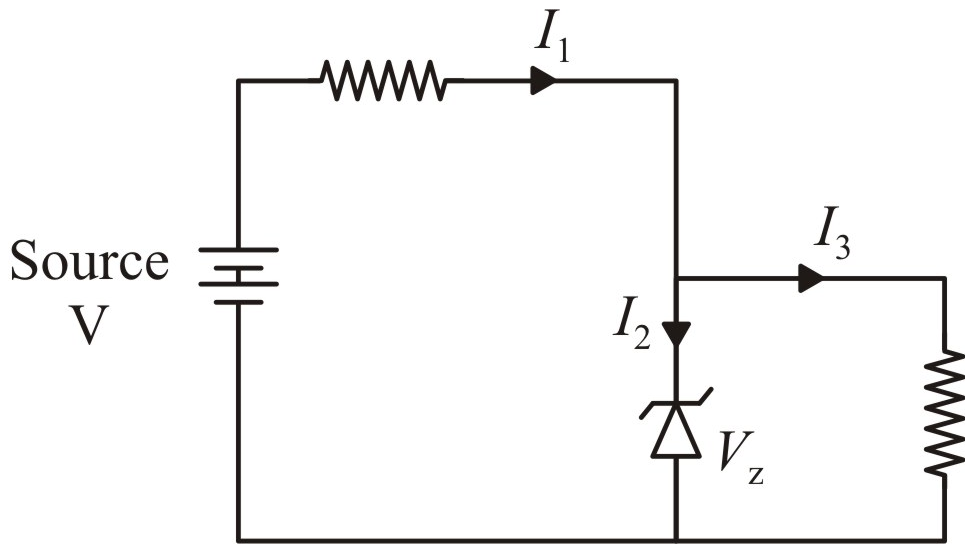
| 1. | all the current \(I_1, I_2~\text{and}~I_3\) change. |
| 2. | only \(I_1\) and \(I_2\) change and \(I_3\) remains constant. |
| 3. | only \(I_1\) and \(I_3\) change and \(I_2\) remains constant. |
| 4. | all the currents remain constant. |
Subtopic: Applications of PN junction |
71%
From NCERT
To view explanation, please take trial in the course.
NEET 2026 - Target Batch - Vital
Hints
To view explanation, please take trial in the course.
NEET 2026 - Target Batch - Vital
The given circuit has two ideal diodes connected as shown in the figure below. The current flowing through the resistance \(R_1\) will be:

| 1. | \(2.5~\text A\) | 2. | \(10.0~\text A\) |
| 3. | \(1.43~\text A\) | 4. | \(3.13~\text A\) |
Subtopic: PN junction |
88%
From NCERT
NEET - 2016
To view explanation, please take trial in the course.
NEET 2026 - Target Batch - Vital
Hints
To view explanation, please take trial in the course.
NEET 2026 - Target Batch - Vital


In the energy band diagram of a material shown below, the open circles and filled circles denote holes and electrons respectively. The material is a/an:

| 1. | \(\mathrm{p}\text-\)type semiconductor |
| 2. | insulator |
| 3. | metal |
| 4. | \(\mathrm{n}\text-\)type semiconductor |
Subtopic: Energy Band theory |
76%
From NCERT
AIPMT - 2007
To view explanation, please take trial in the course.
NEET 2026 - Target Batch - Vital
Hints
To view explanation, please take trial in the course.
NEET 2026 - Target Batch - Vital
Select Chapter Topics:
© 2025 GoodEd Technologies Pvt. Ltd.