- 1(current)
 Q. No.
| Statement I: | Photovoltaic devices can convert optical radiation into electricity. |
| Statement II: | Zener diode is designed to operate under reverse bias in the breakdown. |
| 1. | Statement I is False but Statement II is True. |
| 2. | Both Statement I and Statement II are True. |
| 3. | Both Statement I and Statement II are False. |
| 4. | Statement I is True but Statement II is False. |


| 1. | Zener voltage remains constant at the breakdown. |
| 2. | It is designed to operate under reverse bias. |
| 3. | The depletion region formed is very wide. |
| 4. | \(\mathrm{p}\) and \(\mathrm{n}\) regions of the Zener diode are heavily doped. |
Consider the following statements (A). and (B). and identify the correct answer.
| (A). | A zener diode is connected in reverse bias when used as a voltage regulator. |
| (B). | The potential barrier of p-n junction lies between 0.2 V to 0.3 V. |
| 1. | (A) is correct and (B) is incorrect. |
| 2. | (A) is incorrect and (B) is correct. |
| 3. | (A) and (B) both are correct. |
| 4. | (A) and (B) both are incorrect. |


An LED is constructed from a \(\mathrm{p\text{-}n}\) junction diode using \(\mathrm{GaAsP}\). The energy gap is \(1.9~\text{eV}\). The wavelength of the light emitted will be equal to:
1. \(10.4 \times 10^{-26} \text{m}\)
2. \(654~ \text{nm}\)
3. \(654~ \text{m}\)
4. \(654\times 10^{-11}~\text{m}\)
The given circuit has two ideal diodes connected as shown in the figure below. The current flowing through the resistance \(R_1\) will be:
1. \(2.5~\text{A}\)
2. \(10.0~\text{A}\)
3. \(1.43~\text{A}\)
4. \(3.13~\text{A}\)

The given graph represents the \(\mathrm{V\text{-} I}\) characteristic for a semiconductor device.
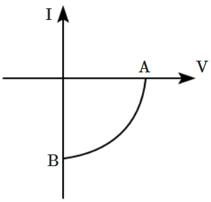
Which of the following statement is correct?
| 1. | It is a \(\mathrm{V\text{-} I}\) characteristic for the solar cell where point \(\mathrm{A}\) represents open-circuit voltage and point \(\mathrm{B}\) short circuit current. |
| 2. | It is for a solar cell and points \(\mathrm{A}\) and \(\mathrm{B}\) represent open-circuit voltage and current, respectively. |
| 3. | It is for a photodiode and points \(\mathrm{A}\) and \(\mathrm{B}\) represent open-circuit voltage and current respectively. |
| 4. | It is for a LED and points \(\mathrm{A}\) and \(\mathrm{B}\) represent open circuit voltage and short circuit current, respectively. |
A Zener diode, having a breakdown voltage equal to 15 V, is used in a voltage regulator circuit as shown in the figure. The current through the diode is:
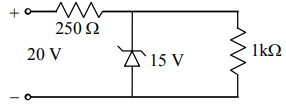
1. 5 mA
2. 10 mA
3. 15 mA
4. 20 mA
A p-n photodiode is made of a material with a bandgap of 2.0 eV. The minimum frequency of the radiation that can be absorbed by the material is nearly:
1.
2.
3.
4.
Zener diode is used for:
1. rectification.
2. stabilisation.
3. amplification.
4. producing oscillations in an oscillator.
Zener diode is used as:
1. Half-wave rectifier
2. Full-wave rectifier
3. A.C. voltage stabilizer
4. D.C. voltage stabilizer
- 1(current)
Q. No.© 2024 GoodEd Technologies Pvt. Ltd.