
 Q. No.


Which of the following-junction is used unbiased?
1. Photo diode
2. LED
3. Zener diode
4. Solar cell


In the given circuit, the power developed in 2 k resistor is:
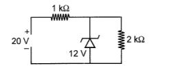
1. 36 mW
2. 12 mW
3. 144 mW
4. 72 mW


The output of the OR gate is 1:
1. only if both inputs are zero.
2. if either or both inputs are 1.
3. only if both inputs are 1.
4. if any of the inputs is zero.
In the circuit shown, are respectively:
(If diodes are ideal)

1. 0, 0
2. 5 mA, 5 mA
3. 5 mA, 0
4. 0, 5 mA
The LED:
1. is reverse-biased.
2. is forward-biased.
3. can be made of GaAs.
4. both (2) & (3) are correct.
Logic gates X and Y have the truth tables shown below:
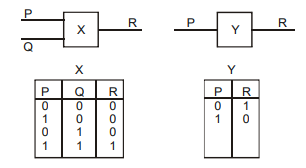
When the output of X is connected to the input of Y, the resulting combination is equivalent to a single:
1. NOT gate
2. OR gate
3. NAND gate
4. AND gate


The depletion layer in the P–N junction region is caused by:
| 1. | the drift of holes |
| 2. | diffusion of charge carriers |
| 3. | migration of impurity ions |
| 4. | drift of electrons |
© 2024 GoodEd Technologies Pvt. Ltd.