
 Q. No.
A potential barrier of 0.50 V exists across a p-n junction. If the depletion region is m wide, the intensity of the electric field in this region is:
1.
\(1.0 \times 10^6 \mathrm{~V} / \mathrm{m}\)
2.
\(1.0 \times 10^5 \mathrm{~V} / \mathrm{m}\)
3.
\(2.0 \times 10^5 \mathrm{~V} / \mathrm{m}\)
4.
\(2.0 \times 10^6 \mathrm{~V} / \mathrm{m}\)


The current through an ideal p-n junction diode shown in the circuit will be:

1. 5 A
2. 0.2 A
3. 0.6 A
4. Zero
Which logic gate is represented by the following combination of logic gates?
1. OR

2. NAND
3. AND
4. NOR


In a p-n junction diode not connected to any circuit:
| 1. | the potential is the same everywhere. |
| 2. | the P-type is at higher potential than the N-type side. |
| 3. | there is an electric field at the junction directed from the N- type side to the P- type side. |
| 4. | there is an electric field at the junction directed from the P-type side to the N-type side. |
When a forward bias is applied to a p-n junction, then what happens to the potential barrier , and the width of charge depleted region x?
| 1. | \(V_B\) increases, x decreases | 2. | \(V_B\) decreases, x increases |
| 3. | \(V_B\) increases, x increases | 4. | \(V_B\) decreases, x decreases |
Which of the energy band diagrams shown in the figure corresponds to that of a semiconductor?
| 1. |  |
2. |  |
| 3. |  |
4. |  |
An LED is constructed from a \(\mathrm{p\text{-}n}\) junction diode using \(\mathrm{GaAsP}\). The energy gap is \(1.9~\text{eV}\). The wavelength of the light emitted will be equal to:
1. \(10.4 \times 10^{-26} \text{m}\)
2. \(654~ \text{nm}\)
3. \(654~ \text{m}\)
4. \(654\times 10^{-11}~\text{m}\)
The energy band diagrams for semiconductor samples of silicon are as shown. We can assert that:

| 1. | sample X is undoped while samples Y and Z have been doped with a third group and a fifth group impurity respectively. |
| 2. | sample X is undoped while both samples Y and Z have been doped with a fifth group impurity. |
| 3. | sample X has been doped with equal amounts of third and fifth group impurities while samples Y and Z are undoped. |
| 4. | sample X is undoped while samples Y and Z have been doped with a fifth group and a third group impurity respectively. |


A Zener diode is shown in the following circuit diagram. When the source voltage fluctuates such that , then:
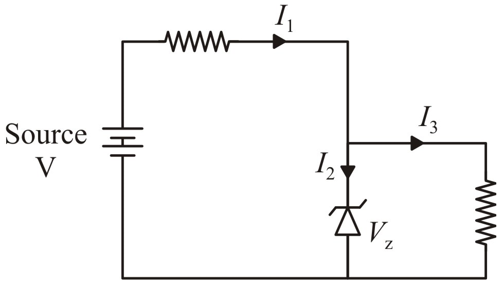
1. all the current I1, I2 and I3 change.
2. only I1 and I2 change and I3 remains constant.
3. only I1 and I3 change and I2 remains constant.
4. all the currents remain constant.
© 2024 GoodEd Technologies Pvt. Ltd.