- 1(current)
 Q. No.
\(\mathrm{C}\) and \(\mathrm{Si}\) both have the same lattice structure, having \(4\) bonding electrons in each. However, \(\mathrm{C}\) is an insulator whereas \(\mathrm{Si}\) is an intrinsic semiconductor. This is because:
| 1. | in the case of \(\mathrm{C},\) the valence band is not completely filled at absolute zero temperature. |
| 2. | in the case of \(\mathrm{C},\) the conduction band is partly filled even at absolute zero temperature. |
| 3. | the four bonding electrons in the case of \(\mathrm{C}\) lie in the second orbit, whereas in the case of \(\mathrm{Si},\) they lie in the third. |
| 4. | the four bonding electrons in the case of \(\mathrm{C}\) lie in the third orbit, whereas for \(\mathrm{Si},\) they lie in the fourth orbit. |


Subtopic: Energy Band theory |
72%
From NCERT
NEET - 2012
To view explanation, please take trial in the course.
NEET 2026 - Target Batch - Vital
Hints
To view explanation, please take trial in the course.
NEET 2026 - Target Batch - Vital

A \(\mathrm{p\text-n}\) photodiode is fabricated from a semiconductor with a band gap of \(2.5~\text{eV}.\) It can detect a signal of wavelength:
1. \(6000~\mathring{A}\)
2. \(4000~\text{nm}\)
3. \(6000~\text{nm}\)
4. \(4000~\mathring{A}\)
1. \(6000~\mathring{A}\)
2. \(4000~\text{nm}\)
3. \(6000~\text{nm}\)
4. \(4000~\mathring{A}\)
Subtopic: Energy Band theory |
64%
From NCERT
AIPMT - 2009
To view explanation, please take trial in the course.
NEET 2026 - Target Batch - Vital
Hints
To view explanation, please take trial in the course.
NEET 2026 - Target Batch - Vital
A p-n photodiode is made of a material with a bandgap of 2.0 eV. The minimum frequency of the radiation that can be absorbed by the material is nearly:
1.
2.
3.
4.
Subtopic: Energy Band theory | Applications of PN junction |
82%
From NCERT
AIPMT - 2008
To view explanation, please take trial in the course.
NEET 2026 - Target Batch - Vital
Hints
To view explanation, please take trial in the course.
NEET 2026 - Target Batch - Vital

In the energy band diagram of a material shown below, the open circles and filled circles denote holes and electrons respectively. The material is a/an:
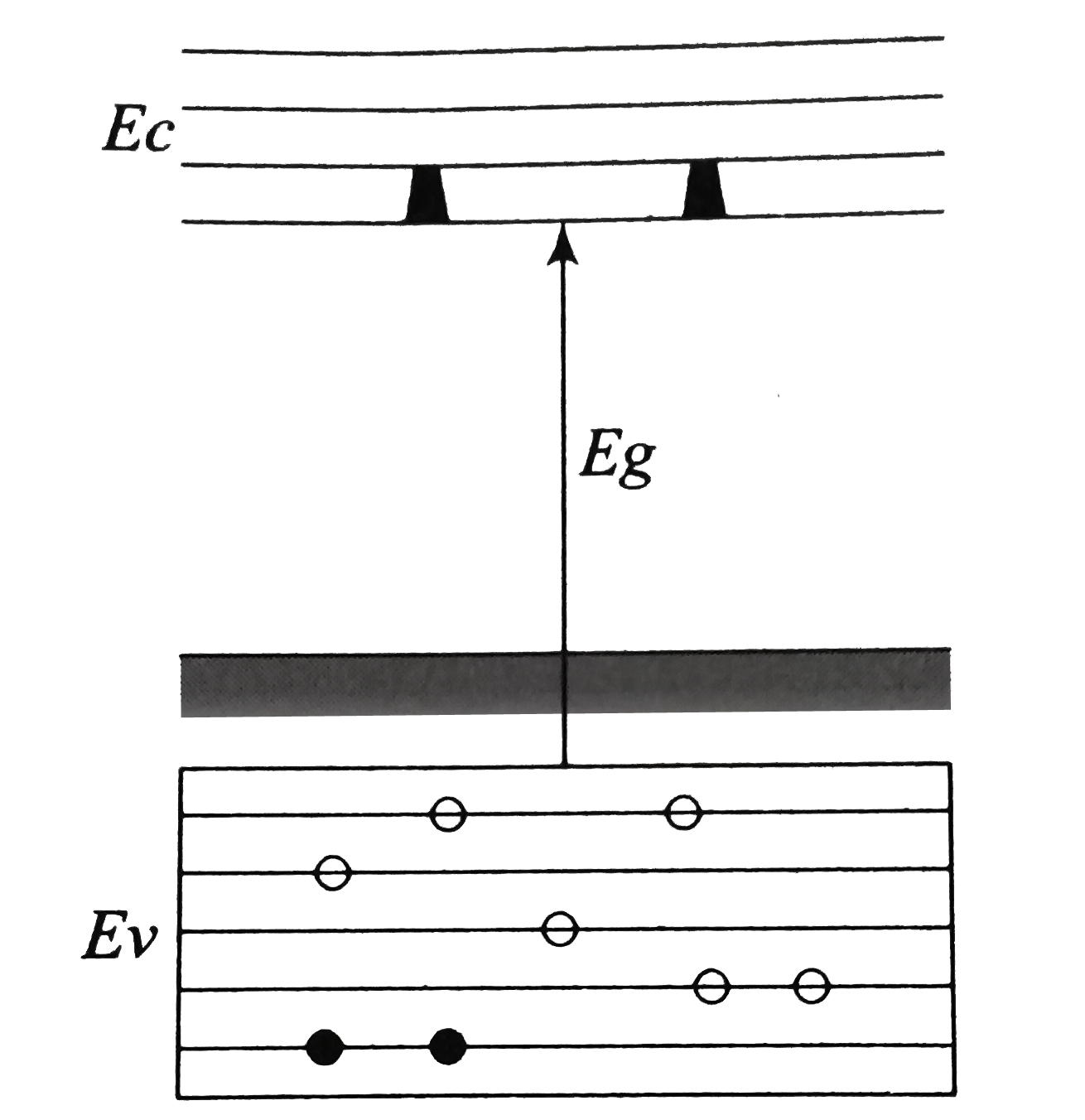
1. p-type semiconductor
2. insulator
3. metal
4. n-type semiconductor
Subtopic: Energy Band theory |
73%
From NCERT
AIPMT - 2007
To view explanation, please take trial in the course.
NEET 2026 - Target Batch - Vital
Hints
To view explanation, please take trial in the course.
NEET 2026 - Target Batch - Vital
- 1(current)
Q. No.© 2025 GoodEd Technologies Pvt. Ltd.