
 Q. No.
A semiconductor is known to have an electron concentration of \(8\times 10^{13}~\text{cm}^{-3},\) and a hole concentration of \(5\times 10^{2}~\text{cm}^{-3}.\) The semiconductor is:
1.
\(\mathrm{n}\text-\)type
2.
\(\mathrm{p}\text-\)type
3.
intrinsic
4.
insulator


To unlock all the explanations of this course, you need to be enrolled.
To unlock all the explanations of this course, you need to be enrolled.

Carbon, Silicon, and Germanium atoms have four valence electrons each. Their valence and conduction bands are separated by energy gaps represented by \(\left(E_g\right)_C,(E_g)_{Si}~\text{and}~(E_g)_{Ge}\) respectively. Which one of the following relationships is true in their case?
1. \(\left(E_g\right)_C<\left(E_g\right)_{G e} \)
2. \(\left(E_g\right)_C>\left(E_g\right)_{S i} \)
3. \(\left(E_g\right)_C=\left(E_g\right)_{S i} \)
4. \(\left(E_g\right)_C<\left(E_g\right)_{S i}\)
To unlock all the explanations of this course, you need to be enrolled.
To unlock all the explanations of this course, you need to be enrolled.
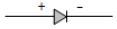
If in a \(\mathrm{p\text-n}\) junction, a square input signal of \(10\) V is applied as shown, then the output across \(R_L\) will be:

| 1. |  |
2. |  |
| 3. |  |
4. |  |
To unlock all the explanations of this course, you need to be enrolled.
To unlock all the explanations of this course, you need to be enrolled.


The given graph represents the \(V\text-I\) characteristics of a semiconductor device. Which of the following statements is correct?

| 1. | It is a \(V\text-I\) characteristic of a solar cell where the point \(A\) represents open-circuit voltage and the point \(B\) represents short-circuit current. |
| 2. | It is for a solar cell and points \(A\) and \(B\) represents open-circuit voltage and current respectively. |
| 3. | It is for a photodiode and points \(A\) and \(B\) represents open-circuit voltage and current respectively. |
| 4. | It is for an LED and points \(A\) and \(B\) represents open-circuit voltage and short-circuit current respectively. |
To unlock all the explanations of this course, you need to be enrolled.
To unlock all the explanations of this course, you need to be enrolled.
| 1. | \(\mathrm{n}\text-\)type with electron concentration \(n_{e}=5\times10^{22}~\text{m}^{-3}\) |
| 2. | \(\mathrm{p}\text-\)type with electron concentration \(n_{e}=2.5\times10^{23}~\text{m}^{-3}\) |
| 3. | \(\mathrm{n}\text-\)type with electron concentration \(n_{e}=2.5\times10^{10}~\text{m}^{-3}\) |
| 4. | \(\mathrm{p}\text-\)type with electron concentration \(n_{e}=5\times10^{9}~\text{m}^{-3}\) |
To unlock all the explanations of this course, you need to be enrolled.
To unlock all the explanations of this course, you need to be enrolled.
The electrical circuit used to get smooth output from a rectifier circuit is called:
1. oscillator.
2. filter.
3. amplifier.
4. logic gates.
To unlock all the explanations of this course, you need to be enrolled.
To unlock all the explanations of this course, you need to be enrolled.


To unlock all the explanations of this course, you need to be enrolled.
To unlock all the explanations of this course, you need to be enrolled.
| 1. | in the case of \(\mathrm{C},\) the valence band is not completely filled at absolute zero temperature. |
| 2. | in the case of \(\mathrm{C},\) the conduction band is partly filled even at absolute zero temperature. |
| 3. | the four bonding electrons in the case of \(\mathrm{C}\) lie in the second orbit, whereas in the case of \(\mathrm{Si},\) they lie in the third. |
| 4. | the four bonding electrons in the case of \(\mathrm{C}\) lie in the third orbit, whereas for \(\mathrm{Si},\) they lie in the fourth orbit. |
To unlock all the explanations of this course, you need to be enrolled.
To unlock all the explanations of this course, you need to be enrolled.
The figure shows a logic circuit with two inputs \(A\) and \(B\) and the output \(C\). The voltage waveforms across \(A\), \(B\), and \(C\) are as given. The logic circuit gate is:

1. \(\text{OR}\) gate
2. \(\text{NOR}\) gate
3. \(\text{AND}\) gate
4. \(\text{NAND}\) gate
To unlock all the explanations of this course, you need to be enrolled.
To unlock all the explanations of this course, you need to be enrolled.

1. \(6000~\mathring{A}\)
2. \(4000~\text{nm}\)
3. \(6000~\text{nm}\)
4. \(4000~\mathring{A}\)
To unlock all the explanations of this course, you need to be enrolled.
To unlock all the explanations of this course, you need to be enrolled.
© 2025 GoodEd Technologies Pvt. Ltd.