In the given figure, the potential difference between \(A\) and \(B\) is:

1.
\(0\)
2.
\(5\) volt
3.
\(10\) volt
4.
\(15\) volt

If in a \(\mathrm{p\text-n}\) junction, a square input signal of \(10\) V is applied as shown, then the output across \(R_L\) will be:
| 1. |  |
2. |  |
| 3. |  |
4. |  |
The given graph represents the \(V\text-I\) characteristics of a semiconductor device. Which of the following statements is correct?

| 1. | It is a \(V\text-I\) characteristic of a solar cell where the point \(A\) represents open-circuit voltage and the point \(B\) represents short-circuit current. |
| 2. | It is for a solar cell and points \(A\) and \(B\) represents open-circuit voltage and current respectively. |
| 3. | It is for a photodiode and points \(A\) and \(B\) represents open-circuit voltage and current respectively. |
| 4. | It is for an LED and points \(A\) and \(B\) represents open-circuit voltage and short-circuit current respectively. |
| 1. | \(\mathrm{n}\text-\)type with electron concentration \(n_{e}=5\times10^{22}~\text{m}^{-3}\) |
| 2. | \(\mathrm{p}\text-\)type with electron concentration \(n_{e}=2.5\times10^{23}~\text{m}^{-3}\) |
| 3. | \(\mathrm{n}\text-\)type with electron concentration \(n_{e}=2.5\times10^{10}~\text{m}^{-3}\) |
| 4. | \(\mathrm{p}\text-\)type with electron concentration \(n_{e}=5\times10^{9}~\text{m}^{-3}\) |
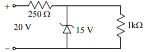
A Zener diode, having breakdown voltage equal to \(15\) V, is used in a voltage regulator circuit, as shown in the figure. The current through the diode is:

1. \(10\) mA
2. \(15\) mA
3. \(20\) mA
4. \(5\) mA
Carbon, Silicon, and Germanium atoms have four valence electrons each. Their valence and conduction bands are separated by energy gaps represented by \(\left(E_g\right)_C,(E_g)_{Si}~\text{and}~(E_g)_{Ge}\) respectively. Which one of the following relationships is true in their case?
1. \(\left(E_g\right)_C<\left(E_g\right)_{G e} \)
2. \(\left(E_g\right)_C>\left(E_g\right)_{S i} \)
3. \(\left(E_g\right)_C=\left(E_g\right)_{S i} \)
4. \(\left(E_g\right)_C<\left(E_g\right)_{S i}\)
| 1. | the current in the reverse biased condition is generally very small. |
| 2. | the current in the reverse biased condition is small but the forward-biased current is independent of the bias voltage. |
| 3. | the reverse-biased current is strongly dependent on the applied bias voltage. |
| 4. | the forward-biased current is very small in comparison to reverse-biased current. |
The electrical circuit used to get smooth output from a rectifier circuit is called:
1. oscillator.
2. filter.
3. amplifier.
4. logic gates.

| 1. | In the circuit (1) and (2) |
| 2. | In the circuit (2) and (3) |
| 3. | In the circuit (1) and (3) |
| 4. | Only in the circuit (1) |
A semiconductor is known to have an electron concentration of \(8\times 10^{13}~\text{cm}^{-3},\) and a hole concentration of \(5\times 10^{2}~\text{cm}^{-3}.\) The semiconductor is:
| 1. | \(\mathrm{n}\text-\)type | 2. | \(\mathrm{p}\text-\)type |
| 3. | intrinsic | 4. | insulator |


