A transistor is operated in a common emitter configuration at Vc =2 V such that a change in the base current from 100 μA to 300 μA produces a change in the collector current from 10 mA to 20mA. The current gain is:

1.  75

2.  100 

3.  25

4.  50

Subtopic:  Transistor (OLD NCERT) |
 76%
From NCERT
AIPMT - 2011
To view explanation, please take trial in the course.
NEET 2023 - Target Batch - Aryan Raj Singh
Hints
To view explanation, please take trial in the course.
NEET 2023 - Target Batch - Aryan Raj Singh

A common emitter amplifier has a voltage gain of 50, an input impedance of 100 Ω and an output impedance of 200 Ω. The power gain of the amplifier is:

1. 500

2. 1000

3. 1250

4. 50

Subtopic:  Applications of Transistor (OLD NCERT) |
 72%
From NCERT
AIPMT - 2010
To view explanation, please take trial in the course.
NEET 2023 - Target Batch - Aryan Raj Singh
Hints
To view explanation, please take trial in the course.
NEET 2023 - Target Batch - Aryan Raj Singh

To get an output Y = 1 from the circuit shown below, the input must be:


1. A=0 B=1 C=0

2. A=0 B=0 C=1

3. A=1 B=0 C=1

4. A=1 B=0 C=0

Subtopic:  Logic gates |
 91%
From NCERT
AIPMT - 2010
To view explanation, please take trial in the course.
NEET 2023 - Target Batch - Aryan Raj Singh
Hints
To view explanation, please take trial in the course.
NEET 2023 - Target Batch - Aryan Raj Singh

p-n photodiode is fabricated from a semiconductor with a band gap of 2.5 eV. It can detect a signal of wavelength:
1. 6000 Å
2. 4000 nm
3. 6000 nm
4. 4000 Å
 
Subtopic:  Energy Band theory |
 63%
From NCERT
AIPMT - 2009
To view explanation, please take trial in the course.
NEET 2023 - Target Batch - Aryan Raj Singh
Hints
To view explanation, please take trial in the course.
NEET 2023 - Target Batch - Aryan Raj Singh

The circuit is equivalent to: 
 The circuit is equivalent to | Physics Questions

1. AND gate

2. NAND gate

3. NOR gate

4. OR gate

Subtopic:  Logic gates |
 75%
From NCERT
AIPMT - 2008
To view explanation, please take trial in the course.
NEET 2023 - Target Batch - Aryan Raj Singh
Hints
To view explanation, please take trial in the course.
NEET 2023 - Target Batch - Aryan Raj Singh

In the following circuit, the output Y for all possible inputs A and B is expressed by the truth table: 


1.
A B Y
0 0 0
0 1 0
1 0 0
1 1 1
2.
A B Y
0 0 1
0 1 1
1 0 1
1 1 0
3.
A B Y
0 0 1
0 1 0
1 0 0
1 1 1
4.
A B Y
0 0 0
0 1 1
1 0 1
1 1 1
Subtopic:  Logic gates |
 75%
From NCERT
AIPMT - 2007
To view explanation, please take trial in the course.
NEET 2023 - Target Batch - Aryan Raj Singh
Hints
To view explanation, please take trial in the course.
NEET 2023 - Target Batch - Aryan Raj Singh

In the energy band diagram of a material shown below, the open circles and filled circles denote holes and electrons respectively. The material is a/an: 

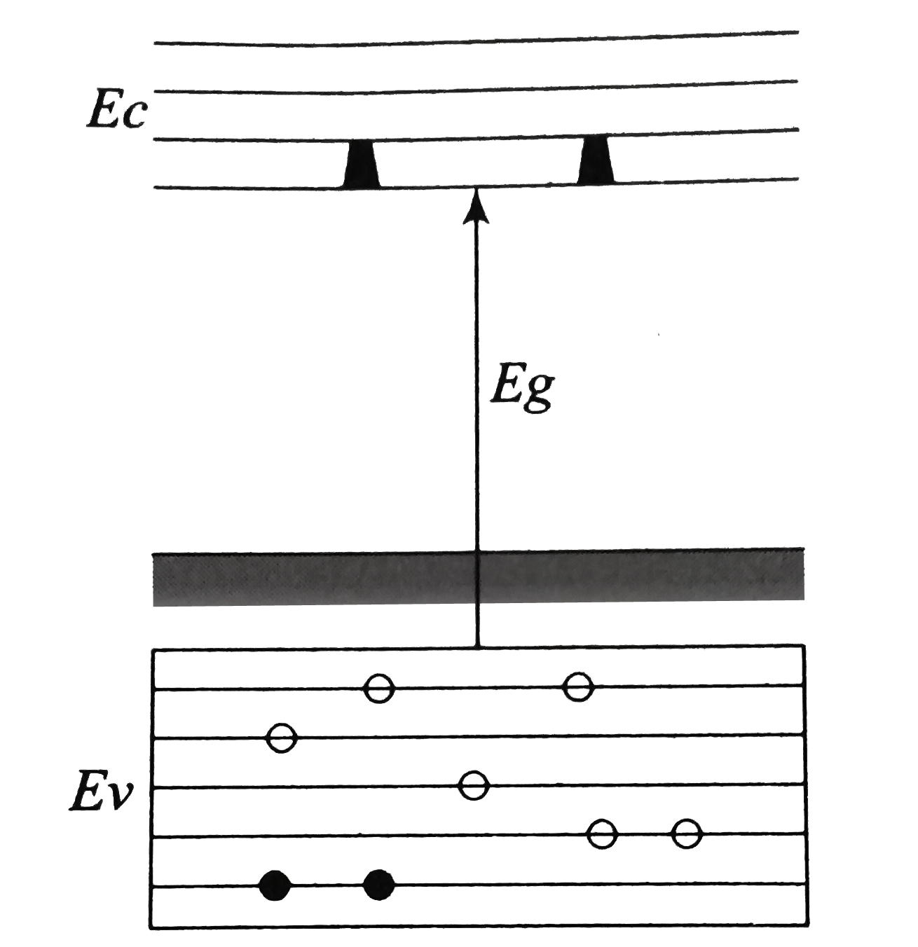
1. p-type semiconductor

2. insulator

3. metal

4. n-type semiconductor

Subtopic:  Energy Band theory |
 72%
From NCERT
AIPMT - 2007
To view explanation, please take trial in the course.
NEET 2023 - Target Batch - Aryan Raj Singh
Hints
To view explanation, please take trial in the course.
NEET 2023 - Target Batch - Aryan Raj Singh

A transistor is operated in a common emitter configuration at constant collector voltage Vc = 1.5 V such that a change in the base current from 100 μA to 150 μA produces a change in the collector current from 5 mA to 10 mA. The current gain (β) is:

1. 67

2. 75

3. 100

4. 50

Subtopic:  Applications of Transistor (OLD NCERT) |
 70%
From NCERT
AIPMT - 2006
To view explanation, please take trial in the course.
NEET 2023 - Target Batch - Aryan Raj Singh
Hints
To view explanation, please take trial in the course.
NEET 2023 - Target Batch - Aryan Raj Singh

Which of the following is an example of forward biasing?
 

1. 2.
3. 4.
Subtopic:  PN junction |
 83%
From NCERT
AIPMT - 2006
To view explanation, please take trial in the course.
NEET 2023 - Target Batch - Aryan Raj Singh
Hints
To view explanation, please take trial in the course.
NEET 2023 - Target Batch - Aryan Raj Singh

The following figure shows a logic gate circuit with two inputs A and B and the output C. The voltage waveforms of A, B, and C are as shown below:
   
The logic circuit gate is:

1. AND gate

2. NAND gate

3. NOR gate

4. OR gate

Subtopic:  Logic gates |
 75%
From NCERT
AIPMT - 2006
To view explanation, please take trial in the course.
NEET 2023 - Target Batch - Aryan Raj Singh
Hints
To view explanation, please take trial in the course.
NEET 2023 - Target Batch - Aryan Raj Singh