
 Q. No.
The circuit diagram shown here corresponds to the logic gate:

1. \(\text{NOR}\)
2. \(\text{AND}\)
3. \(\text{OR}\)
4. \(\text{NAND}\)
1. \(\text{NOR}\)
2. \(\text{AND}\)
3. \(\text{OR}\)
4. \(\text{NAND}\)


An LED is constructed from a \(\mathrm{p\text{-}n}\) junction diode using \(\mathrm{GaAsP}.\) The energy gap is \(1.9~\text{eV}.\) The wavelength of the light emitted will be equal to:
1. \(10.4 \times 10^{-26}~ \text{m}\)
2. \(654~ \text{nm}\)
3. \(654~ \text{m}\)
4. \(654\times 10^{-11}~\text{m}\)
The correct Boolean operation represented by the circuit diagram given above is:
1. \(\mathrm{NOR}\)
2. \(\mathrm{AND}\)
3. \(\mathrm{OR}\)
4. \(\mathrm{NAND}\)


The following figure shows a logic gate circuit with two inputs A and B and the output C. The voltage waveforms of A, B, and C are as shown below:
The logic circuit gate is:

1. AND gate
2. NAND gate
3. NOR gate
4. OR gate


A transistor is operated in a common emitter configuration at constant collector voltage Vc = 1.5 V such that a change in the base current from 100 μA to 150 μA produces a change in the collector current from 5 mA to 10 mA. The current gain (β) is:
1. 67
2. 75
3. 100
4. 50


In the energy band diagram of a material shown below, the open circles and filled circles denote holes and electrons respectively. The material is a/an:
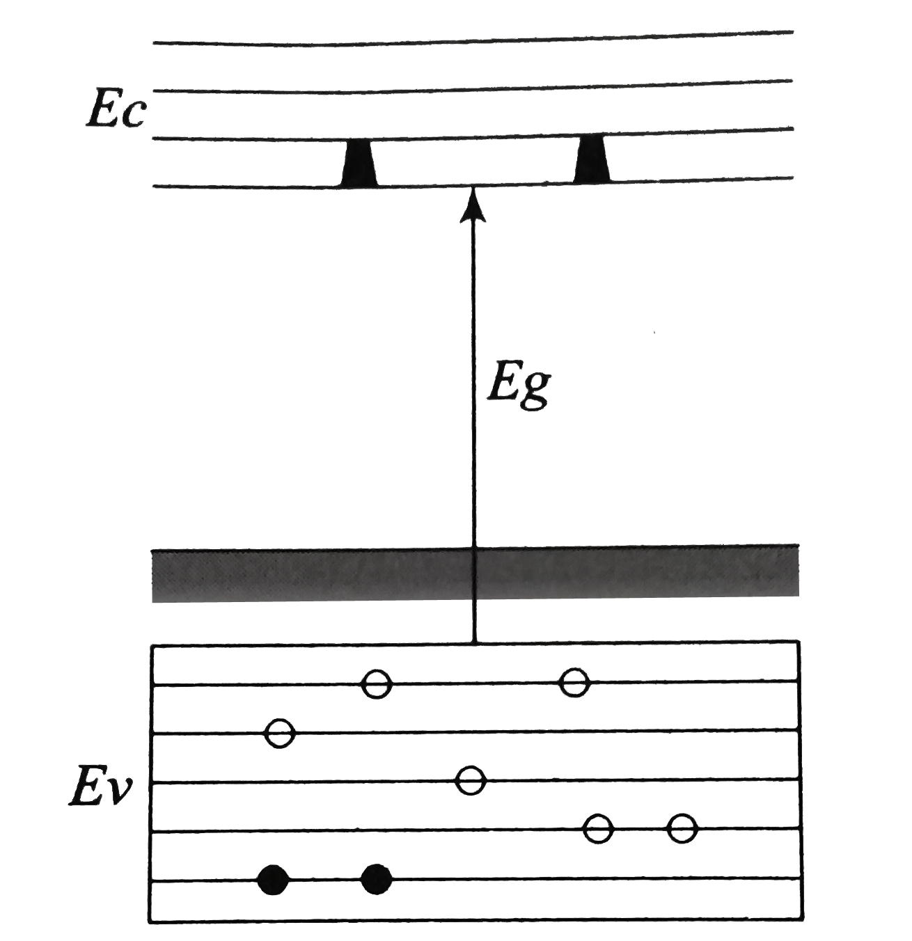
1. p-type semiconductor
2. insulator
3. metal
4. n-type semiconductor
In the following circuit, the output \(Y\) for all possible inputs \(A\) and \(B\) is expressed by the truth table:

| 1. | A | B | Y | 2. | A | B | Y |
| 0 | 0 | 0 | 0 | 0 | 1 | ||
| 0 | 1 | 0 | 0 | 1 | 1 | ||
| 1 | 0 | 0 | 1 | 0 | 1 | ||
| 1 | 1 | 1 | 1 | 1 | 0 | ||
| 3. | 0 | 0 | 1 | 4. | 0 | 0 | 0 |
| 0 | 1 | 0 | 0 | 1 | 1 | ||
| 1 | 0 | 0 | 1 | 0 | 1 | ||
| 1 | 1 | 1 | 1 | 1 | 1 |


1. \(6000~\mathring{A}\)
2. \(4000~\text{nm}\)
3. \(6000~\text{nm}\)
4. \(4000~\mathring{A}\)
© 2026 GoodEd Technologies Pvt. Ltd.