The following configuration of the logic gate is equivalent to
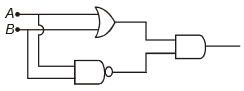
1. NAND gate
2. XOR gate
3. OR gate
4. NOR gate
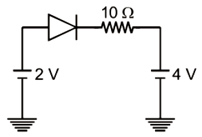
Three ideal diodes are connected to the battery as shown in the circuit. The current supplied by the battery is:
1. zero
2. \(4~\text{A}\)
3. \(2~\text{A}\)
4. \(6~\text{A}\)
If a small amount of aluminium is added to the silicon crystal:
| 1. | its resistance decreases. |
| 2. | it becomes a \(\mathrm{p\text-}\)type semiconductor. |
| 3. | there will be fewer free electrons than holes in the semiconductor. |
| 4. | All of these are correct. |
| 1. | the depletion region becomes thick. |
| 2. | the \(\mathrm{p}\text-\)side is at a higher potential than \(\mathrm{n\text-}\)side. |
| 3. | the current flowing is zero. |
| 4. | the effective resistance is of the order of \(10^6 ~\Omega\). |
When a transistor is used as a switch it is in:
1. Active state
2. Cut off state
3. Saturation state
4. Both cut off state and saturation state are possible
For a transistor amplifier, the power gain and voltage gain are 150 and 10 respectively. The current gain is-
1.
2.
3. 15
4. 1500
When the temperature of the silicon sample is increased from to , the conductivity of silicon will be
1. Increased
2. Decreased
3. Remain same
4. Zero
A transistor is used in common emitter mode in an amplifier circuit. When a signal of 10 mV is added to the base-emitter voltage, the base current changes by 15 A and the collector current changes by 1.5 mA. The current gain b will be
1. 50
2. 48
3. 100
4. 200
The current through an ideal p-n junction diode shown in the circuit will be:
1. 5 A
2. 0.2 A
3. 0.6 A
4. zero

1. 36 mW
2. 12 mW
3. 144 mW
4. 64 mW
Following diagram performs logic function of
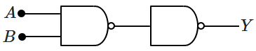
1. AND gate
2. NAND gate
3. XOR gate
4. OR gate
The given electrical network is equivalent to
1. AND gate
2. OR gate
3. NOR gate
4. NOT gate
Which one of the following represents forward biased circuit?
1.
2.
3.
4.
What is the output Y in the following circuit, when all the three inputs A,B,C are first 0 and then 1 ?
1. 0,1
2. 0,0
3. 1,0
4. 1,1
In the given figure, a diode D is connected to an external resistance R = 100 Ω and an e.m.f of 3.5 V. If the barrier potential developed across the diode is 0.5 V, the current in the circuit will be
1. 30mA
2. 40mA
3. 20mA
4. 35mA
The barrier potential of a p-n junction depends on
(i)type of semiconductor material
(ii)amount of doping
(iii)temperature
Which one of the following is correct
1. (i) and (ii)only
2. (ii) only
3. (ii) and (iii)only
4. (i),(ii) and (iii)
In a CE transistor amplifier, the audio signal voltage across the collector resistance of 2 If the base resistance is 1 and the current amplification of the transistor is 100, the input signal voltage is
1. 0.1 V
2. 1.0 V
3. 1mV
4. 10mV
C and Si both have same lattice structure,having 4 bonding electrons in each.However, C is insulator whereas Si is intrinsic semiconductor. This is because
1. in case of C, the valence band is not completely filled at absolute zero temperature
2. in case of C,the condition band is partly filled even at absolute zero temperature
3. the four bonding electrons in the case of C lie in the second orbit,Whereas in the case of Si they lie in the third
4 .the four bonding electrons in the case of C lie in the third orbit, whereas for Si they lie in the fourth orbit
The figure shows a logic circuit with two inputs A and B and the output C. The voltage wave forms across A, B and C are as given. The logic circuit gate is
1. OR gate
2. NOR gate
3. AND gate
4. NAND gate
The input resistance of a silicon transistor is
100 . Base current is changed by 40
which results in a change in collector current
by 2 mA. This transistor is used as a common-
emitter amplifier with a load resistance of 4 k.
The voltage gain of the amplifier is
1. 2000
2. 3000
3. 4000
4. 1000
To get an output Y=1 in given circuit, which
of the following input will be correct ?
A B C
1. 1 0 0
2. 1 0 1
3. 1 1 0
4. 0 1 0
A transistor is operated in common emitter configuration at such that a change in the base current from to produces a change in the collector current from to . The current gain is
1. 75 2. 100
3. 25 4. 50
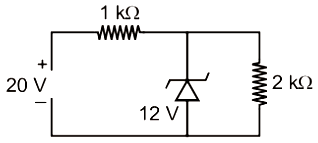
A Zener diode, having breakdown voltage equal to \(15\) V, is used in a voltage regulator circuit, as shown in the figure. The current through the diode is:
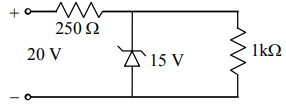
1. \(10\) mA
2. \(15\) mA
3. \(20\) mA
4. \(5\) mA
The device that can act as a complete electronic circuit is
1. Junction diode
2. Integrated circuit
3. Junction transistor
4. Zener diode
A transistor is operated in common-emitter configuration at such that a change in the base current from 100 to 200 produces a change in the collector current from 5 mA to 10 mA. The current gain is
1. 75
2. 100
3. 150
4. 50
A p-n photodiode is made of a material with a band gap of 2.0 eV. The minimum frequency of the radiation that can be absorbed by the material is nearly
1.
2.
3.
4.
The circuit is equivalent to
1. AND gate 2. NAND gate
3. NOR gate 4. OR gate
| 1. | the current in the reverse biased condition is generally very small. |
| 2. | the current in the reverse biased condition is small but the forward-biased current is independent of the bias voltage. |
| 3. | the reverse-biased current is strongly dependent on the applied bias voltage. |
| 4. | the forward-biased current is very small in comparison to reverse-biased current. |
The reverse biasing in a PN junction diode
1. Decreases the potential barrier
2. Increases the potential barrier
3. Increases the number of minority charge carriers
4. Increases the number of majority charge carriers
The electrical resistance of depletion layer is large because:
1. It has no charge carriers
2. It has a large number of charge carriers
3. It contains electrons as charge carriers
4. It has holes as charge carriers
In an NPN transistor the collector current is 24 mA. If 80% of electrons reach collector its base current in mA is
1. 36 2. 26
3. 16 4. 6
In the circuit shown in the figure, the maximum output voltage is :
1. 0 V 2. 5 V
3. 10 V 4.
A semi-conducting device is connected in a series in the circuit with a battery and resistance. A current is allowed to pass through the circuit. If the polarity of the battery is reversed, the current drops to almost zero. The device maybe
(1) a pn junction
(2) an intrinsic semiconductor
(3) a p-type semiconductor
(4) an n-type semiconductor
Which one of the following gates will have an output of 1?
(A)
(B)
(C)
(D)
(1) A
(2) B
(3) C
(4) D
The truth table given below is for which gate?
|
Input |
Output |
|
|
A |
B |
C |
|
0 |
0 |
1 |
|
0 |
1 |
1 |
|
1 |
0 |
1 |
|
1 |
1 |
0 |
(1) XOR
(2) OR
(3) AND
(4) NAND
The following circuit represents:
(1) OR gate
(2) XOR gate
(3) AND gate
(4) NAND gate
In which of the following figures junction diode is forward biased?
(1)
(2)
(3)
(4)
If the internal resistance of the cell is negligible, then current flowing through the circuit is
(1)
(2)
(3)
(4)
For a transistor , then, the current gain for common emitter configuration
(1) 12
(2) 6
(3) 48
(4) 24
For which logic gate, the given truth table is shown?
A B Y
1 1 0
0 1 1
1 0 1
0 0 1
(1) NAND
(2) XOR
(3) NOR
(4) OR
Following diagram performs the logic function of
(1) AND gate
(2) NAND gate
(3) OR gate
(4) XOR gate
Which one of the diode is reverse biased?
(1)
(2)
(3)
(4)
Application of forward bias to a p-n junction
(1) widens the depletion zone
(2) increases the number of donors on the n-side
(3) increases the potential difference across the depletion zone
(4) increases the electric field in the depletion zone
In a p-n junction photocell, the value of the photo electromotive force produced by monochromatic light is proportional to
(1) the intensity of the light falling on the cell
(2) the frequency of the light falling on the cell
(3) the voltage applied at the p-n junction
(4) the barrier voltage at the p-n junction
A transistor is operated in common emitter configuration at constant voltage such that a change in the base current from 100 to 150 produces a change in the collector current from 5 to 10 mA. The current gain () is
(1) 67
(2) 75
(3) 100
(4) 50


