To get output \(Y = 1\) in the given circuit which of the following input will be correct?


\(A\) \(B\) \(C\)
1. 1 0 1
2. 1 1 0
3. 0 1 0
4. 1 0 0

Subtopic:  Logic gates |
 91%
From NCERT
AIPMT - 2012
To view explanation, please take trial in the course.
NEET 2023 - Target Batch - Aryan Raj Singh
Hints
To view explanation, please take trial in the course.
NEET 2023 - Target Batch - Aryan Raj Singh

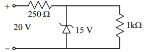
A Zener diode, having a breakdown voltage equal to 15 V, is used in a voltage regulator circuit as shown in the figure. The current through the diode is:

1. 5 mA
2. 10 mA
3. 15 mA
4. 20 mA

Subtopic:  Applications of PN junction |
 65%
From NCERT
AIPMT - 2011
To view explanation, please take trial in the course.
NEET 2023 - Target Batch - Aryan Raj Singh
Hints
To view explanation, please take trial in the course.
NEET 2023 - Target Batch - Aryan Raj Singh

In the following figure, the diodes which are forward biased are:
 

(a)
(b)
(c)
(d)
 

1. (a), (b) and (d)
2. (c) only
3. (a) and (c)
4. (b) and (d)

Subtopic:  PN junction |
 83%
From NCERT
AIPMT - 2011
To view explanation, please take trial in the course.
NEET 2023 - Target Batch - Aryan Raj Singh
Hints
To view explanation, please take trial in the course.
NEET 2023 - Target Batch - Aryan Raj Singh

Pure Si at \(500~\text{K}\) has an equal number of electron \((n_e)\) and hole\((n_h)\) concentrations of \(1.5\times10^{16}~\text{m}^{-3}\). Doping by indium increases \(n_h\) to \(4.5\times10^{22}~\text{m}^{-3}\).  The doped semiconductor is of:

1. \(p\)-type with electron concentration \(n_e=5\times10^9~\text{m}^{-3}\)
2. \(n\)-type with electron concentration \(n_e=5\times10^{22}~\text{m}^{-3}\)
3. \(p\)-type with electron concentration \(n_e=2.5\times10^{10}~\text{m}^{-3}\) 
4. \(n\)-type with electron concentration \(n_e=2.5\times10^{23}~\text{m}^{-3}\)
Subtopic:  Types of Semiconductors |
 76%
From NCERT
AIPMT - 2011
To view explanation, please take trial in the course.
NEET 2023 - Target Batch - Aryan Raj Singh
Hints
To view explanation, please take trial in the course.
NEET 2023 - Target Batch - Aryan Raj Singh

The following figure shows a logic gate circuit with two inputs A and B, and the output Y. The voltage waveforms of A, B and Y are as given.
 

The logic gate is:

1. OR gate

2. AND gate

3. NAND gate

4. NOR gate

Subtopic:  Logic gates |
 79%
From NCERT
AIPMT - 2010
To view explanation, please take trial in the course.
NEET 2023 - Target Batch - Aryan Raj Singh
Hints
To view explanation, please take trial in the course.
NEET 2023 - Target Batch - Aryan Raj Singh

The output from a \(\mathrm{NAND}\) gate is divided into two in parallel and fed to another \(\mathrm{NAND}\) gate. The resulting gate is a:

 
1. \(\mathrm{AND}\) gate
2. \(\mathrm{NOR}\) gate
3. \(\mathrm{OR}\) gate
4. \(\mathrm{NOT}\) gate
Subtopic:  Logic gates |
 79%
From NCERT
NEET - 2013
Please attempt this question first.
Hints
Please attempt this question first.

In an unbiased \(\mathrm{p\text{-}n}\) junction, holes diffuse from the \(\mathrm{p\text{-}}\)regions to \(\mathrm{n\text{-}}\)regions because of: 
1. the attraction of free electrons of the \(\mathrm{n\text{-}}\)region.
2. the higher hole concentration in the \(\mathrm{p\text{-}}\)region than that in the \(\mathrm{n\text{-}}\)region. 
3. the higher concentration of electrons is in the \(\mathrm{p\text{-}}\)region than that in the \(\mathrm{n\text{-}}\)region. 
4. the potential difference across the \(\mathrm{p\text{-}n}\) junction. 
Subtopic:  PN junction |
 65%
From NCERT
NEET - 2013
Please attempt this question first.
Hints
Please attempt this question first.

The following figure shows a logic gate circuit with two inputs A and B and the output C. The voltage waveforms of A, B, and C are as shown below:
   
The logic circuit gate is:

1. AND gate

2. NAND gate

3. NOR gate

4. OR gate

Subtopic:  Logic gates |
 75%
From NCERT
AIPMT - 2006
To view explanation, please take trial in the course.
NEET 2023 - Target Batch - Aryan Raj Singh
Hints
To view explanation, please take trial in the course.
NEET 2023 - Target Batch - Aryan Raj Singh

Which of the following is an example of forward biasing?
 

1. 2.
3. 4.
Subtopic:  PN junction |
 83%
From NCERT
AIPMT - 2006
To view explanation, please take trial in the course.
NEET 2023 - Target Batch - Aryan Raj Singh
Hints
To view explanation, please take trial in the course.
NEET 2023 - Target Batch - Aryan Raj Singh

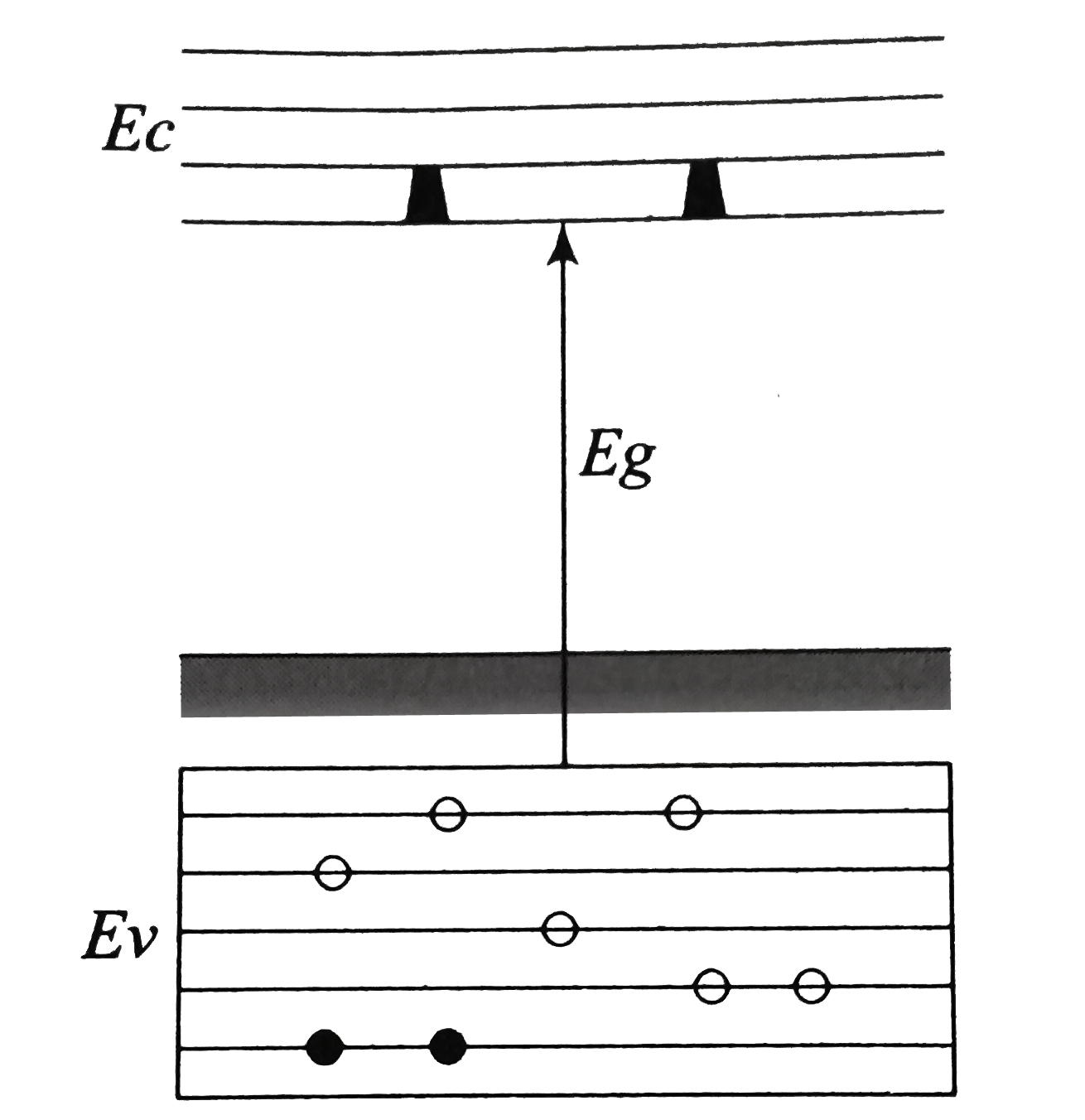
In the energy band diagram of a material shown below, the open circles and filled circles denote holes and electrons respectively. The material is a/an: 
1. p-type semiconductor

2. insulator

3. metal

4. n-type semiconductor

Subtopic:  Energy Band theory |
 72%
From NCERT
AIPMT - 2007
To view explanation, please take trial in the course.
NEET 2023 - Target Batch - Aryan Raj Singh
Hints
To view explanation, please take trial in the course.
NEET 2023 - Target Batch - Aryan Raj Singh